4.3.10. LPWM Driver Debug Guide
4.3.10.1. Overview
LPWM (Lite-PWM) is used to generate square waves with variable pulse width and frequency, synchronized with PPS trigger signals. It is typically used in the camsys system to trigger sensor exposure. The LPWM itself also requires external triggering; upon receiving a trigger signal, it outputs square waves according to the configured LPWM parameters.
Parameter Specifications:
The default supported frequency range of LPWM is 1Hz - 1MHz, with output pulse width ranging from 1μs to 4ms.
4.3.10.2. Features
The LPWM module in the chip has the following characteristics:
1. Contains two independent LPWM COREs, each with programmable period and sampling period.
2. Each LPWM CORE includes 4 channel outputs.
3. LPWM supports two different triggering modes: external hardware trigger and internal software trigger.
4. Each LPWM channel can be individually enabled or disabled.
5. The polarity of the pulse for each LPWM channel can be selected via software.
4.3.10.3. Functional Description
Typical Applications
When using multiple Camera Sensors, LPWM is required to control the FSIN/VSYNC pins to achieve synchronized capture across multiple sensors. There are mainly three control methods:
Method 1:
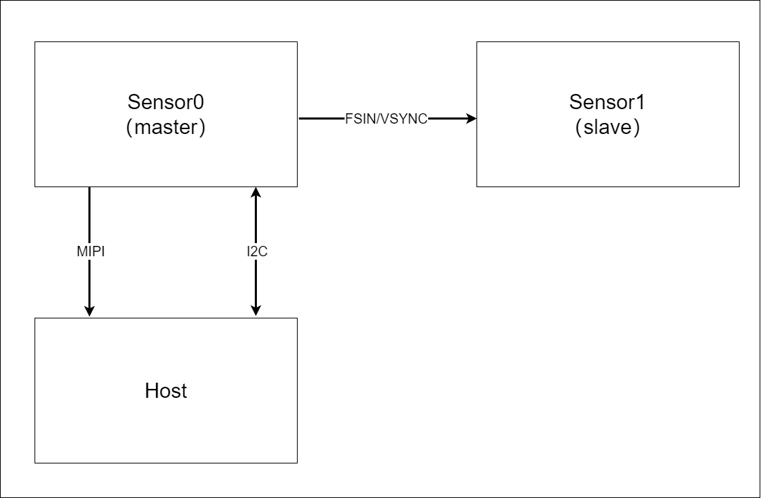
Sensor0 is configured as master mode (FSIN/VSYNC as output), while Sensor1 is configured as slave mode (FSIN/VSYNC as input).
Sensor0 acts as the master device, outputting the FSYNC signal to synchronize other sensors. When the HOST initiates image capture, Sensor0 outputs an FSYNC signal during its exposure period, triggering other sensors to perform synchronized capture.
The FSIN/VSYNC pin of Sensor1 is set as input and controlled by Sensor0, thereby achieving synchronized capture between the two image sensors.
Method 2:
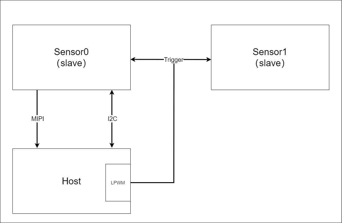
Both sensors are configured in slave mode, so each frame capture is triggered by an external FSYNC signal.
The HOST sends a synchronization signal uniformly to the Slave Sensors to trigger their exposure. Based on the configured LPWM parameters, a square wave signal is output on the trigger pin. Whenever both sensors receive the trigger signal, they simultaneously capture one frame of image.
Method 3:
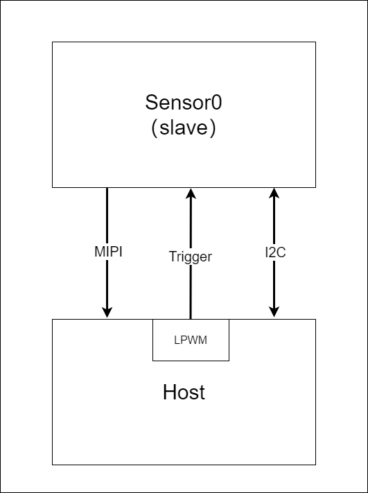
One sensor is configured in Slave mode. When the HOST initiates image capture, a square wave based on the LPWM configuration is output on the trigger pin. Upon receiving the trigger signal, the sensor captures one frame of image.
Functional Principle
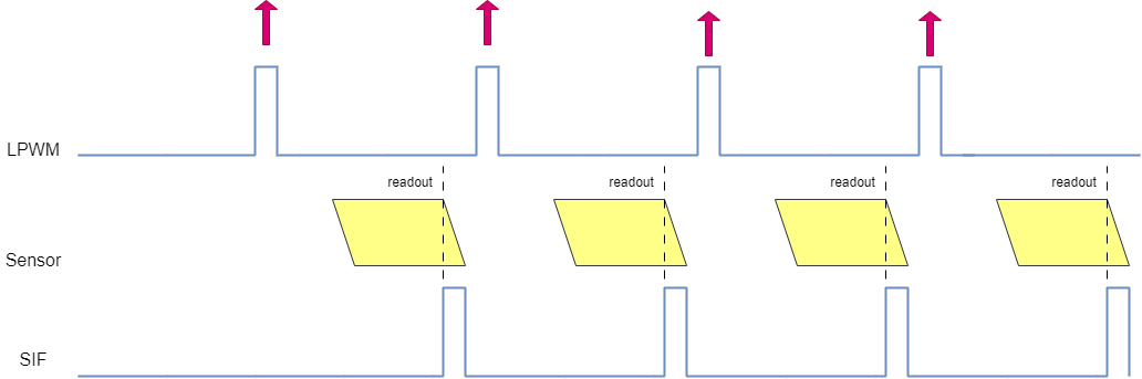
The LPWM_CORE module generates output waveforms according to user configuration, allowing customization of period, duty cycle, and offset. The LPWM core divides the reference clock (clk_lpwm) to generate a 1MHz working clock. An internal time counter calculates time ticks and generates pulses with user-defined offset, period, and width. Each LPWM CORE can operate independently according to its configuration, as shown in the timing diagram below:
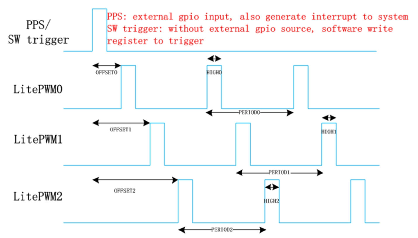
When the sensor receives the LPWM trigger signal (red arrow), it starts exposure and image output. However, due to a fixed delay inherent in the LPWM that persists throughout operation, the trigger signal is not perfectly aligned with SIF exposure output. The interaction between LPWM, Sensor, and SIF is illustrated below:
4.3.10.4. Driver Code
LPWM Code Path
kernel/drivers/media/platform/horizon/camsys/lpwm/
Kernel Configuration
/* arch/arm64/configs/hobot_x5_soc_defconfig */
..
CONFIG_HOBOT_LPWM=m
...
DTS Node Configuration
The X5 PWM and LPWM controller device tree definitions are located in arch/arm64/boot/dts/hobot/x5.dtsi under the kernel directory. To enable specific PWM port outputs, modify the corresponding board-level file. Taking x5-evb.dts as an example, enable lpwm0 ch0-4 and lpwm1 ch1.
Note: Nodes in x5.dtsi mainly declare SoC common features and are unrelated to specific circuit boards; generally, they should not be modified.
/* arch/arm64/boot/dts/hobot/x5-evb.dts */
...
&lpwm0 {
	status = "okay";
	/* conflict with camera pwd gpio */
	pinctrl-names = "default";
	pinctrl-0 = <&pinctrl_lpwm0_0 &pinctrl_lpwm0_1
			&pinctrl_lpwm0_2 &pinctrl_lpwm0_3>;
};


&lpwm1 {
	status = "okay";
	pinctrl-names = "default";
	/** for display backlight **/
	pinctrl-0 = <&pinctrl_lpwm1_1>;
};
...
Explanation of LPWM device tree nodes:
&lpwm0: This is a device node representing a PWM controller named lpwm0.status = "okay": Indicates enabling this device node, meaning the lpwm0 PWM controller is active. If set to “disabled”, the device will be disabled.pinctrl-names = "default": Defines the name of the pin control configuration, using the default pin control setup here.pinctrl-0 = <&pinctrl_lpwm0_0 &pinctrl_lpwm0_1 &pinctrl_lpwm0_2 &pinctrl_lpwm0_3>: Enables four channels of LPWM0.Specifies the pin configuration for the lpwm0 controller. This is an array of pointers to a series of pin control configurations (typically managed by the pinctrl subsystem). Each
pinctrl_lpwm0_Xrepresents a predefined pin configuration used to control the behavior of LPWM signals on physical pins, such as pin number, multiplexing function, power domain settings, etc.
4.3.10.5. Function Usage
Kernel Space
LPWM Probe Driver Source Code
The hobot_lpwm_probe function is an initialization function for a device driver, part of the platform_driver’s probe operation. It executes when the device is detected and the driver is loaded, used to initialize LPWM module hardware resources and configure the platform device.
static int32_t hobot_lpwm_probe(struct platform_device *pdev)
{
	int32_t ret = LPWM_RET_OK;
	struct hobot_lpwm_ins *lpwm;

	lpwm = (struct hobot_lpwm_ins *)osal_kmalloc(sizeof(struct hobot_lpwm_ins),0);
	if (IS_ERR(lpwm)) {
		lpwm_err(NULL, "devm kzalloc failed!\n");
		return -ENOMEM;
	}
	memset(lpwm, 0, sizeof(struct hobot_lpwm_ins));

	ret = lpwm_preinit(pdev, lpwm);
	if (ret != LPWM_RET_OK) {
		return ret;
	}

	ret = lpwm_platform_init(pdev, lpwm);
	if (ret != LPWM_RET_OK) {
		goto err_disable_clk;
	}

	ret = pwmchip_add(&lpwm->chip);
	if (ret < 0) {
		lpwm_err(lpwm, "Add to Linux pwm chip failed!\n");
		goto err_free_irq;
	}

	ret = lpwm_sysfs_create(pdev);
	if (ret < 0) {
		lpwm_err(lpwm, "Sysfs create failed!\n");
		goto err_free_pwm_chip;
	}

	platform_set_drvdata(pdev, lpwm);
	ret = lpwm_chip_cdev_create(lpwm);
	if (ret != LPWM_RET_OK) {
		goto err_free_pwm_chip;
	}

	lpwm_div_ratio_config(lpwm->base, 24);
	glpwm_chip[lpwm->dev_idx] = lpwm;
	lpwm->cim_cops = vio_get_callback_ops(&cim_ops, VIN_MODULE, COPS_9);

	vin_register_device_node(VIN_LPWM, &vin_lpwm_ops);
	lpwm_info(lpwm, "Probe success\n");

	return ret;

err_free_pwm_chip:
	pwmchip_remove(&lpwm->chip);
err_free_irq:
	devm_free_irq(&pdev->dev, lpwm->irq, lpwm);
err_disable_clk:
	clk_disable_unprepare(lpwm->sclk);
	clk_disable_unprepare(lpwm->pclk);
	osal_kfree(lpwm);
	return ret;
}
Driver Source Code Interfaces
1. osal_kmalloc
Function: Used in
hobot_lpwm_probeto allocate memory for an instance of typestruct hobot_lpwm_ins.Parameters: The first parameter is the size of memory to allocate; the second parameter is usually memory allocation flags (0 means default).
Return Value: Returns the allocated memory address; returns NULL if allocation fails.
2. lpwm_preinit
Function: Performs pre-initialization of the LPWM device.
Parameters: Platform device object (pdev) and LPWM device object (lpwm).
Return Value: Returns a status code; LPWM_RET_OK indicates successful initialization.
3. lpwm_platform_init
Function: Initializes hardware resources required by the LPWM driver, such as clocks, GPIOs, IRQs, etc.
Parameters: Platform device object (pdev) and LPWM device object (lpwm).
Return Value: Returns a negative value for failure, 0 for success.
4. pwmchip_add
Function: Creates a pwmchip object for the device and adds the LPWM device to the Linux kernel’s PWM subsystem.
Parameters:
&lpwm->chipis the PWM configuration structure for the LPWM device.Return Value: Returns a negative value for failure, 0 for success.
5. lpwm_sysfs_create
Function: Creates files related to LPWM in sysfs, allowing user space to interact with the driver through the file system.
Parameters: LPWM device object (lpwm).
Return Value: Returns LPWM_RET_OK for success, others indicate failure.
6. lpwm_chip_cdev_create
Function: Creates a character device for the LPWM device, allowing applications to access it via device files.
Parameters: Clock handle.
Return Value: Returns the callback operation structure.
7. vio_get_callback_ops
Function: Retrieves callback operations related to VIN (Video Input).
Parameters: Callback operation structure (&cim_ops), module identifier (VIN_MODULE), operation type identifier (COPS_9).
Return Value: Returns the reset controller handle; returns ERR_PTR if retrieval fails.
8. vin_register_device_node
Function: Registers the LPWM device into the VIN subsystem as a video input device.
Parameters: Device type identifier (VIN_LPWM), callback operation structure (&vin_lpwm_ops).
Return Value: None.
The hobot_lpwm_probe function uses vin_register_device_node(VIN_LPWM, &vin_lpwm_ops) to register a video input-related device (in this case, LPWM) into the VIN framework. vin_common_ops is a structure defining a set of operations related to video input devices, where each operation function corresponds to a specific video input control operation:
static struct vin_common_ops vin_lpwm_ops = {
    .open = lpwm_open,
    .close = lpwm_close,
    .video_set_attr = lpwm_init,
    .video_get_attr = lpwm_get_attr,
    .video_set_attr_ex = lpwm_change_attr,
    .video_start = lpwm_start,
    .video_stop = lpwm_stop,
    .video_reset = lpwm_reset,
};
User Space
LPWM Configuration and Usage Instructions
Taking SC230AI software triggering as an example, the LPWM configuration file can be found at app/samples/platform_samples/vp_sensors/sc230ai/linear_1920x1080_raw10_10fps_1lane.c.
.lpwm_attr = {
	.enable = 0,
	.lpwm_chn_attr = {
		{	.trigger_source = 0,
			.trigger_mode = 0,
			.period = 100*1000,
			.offset = 10,
			.duty_time = 100,
			.threshold = 0,
			.adjust_step = 0,
		},
	},
};
Explanation of lpwm_attr structure parameters:
| Parameter | Description | Range | Output 30Hz, High Level 10μs Parameters |
|---|---|---|---|
| offset | Time offset relative to the trigger point | 11 | |
| duty_time | Active high time; actual effective time is (duty_time + 1)μs | [0, 4000 | period) μs | 9 |
| period | Period; actual effective period is (period + 1)μs | [1, 1000000) μs | 33332 |
| threshold | Threshold for gradual synchronization function | [0, 65535] μs | 0 |
| adjust_step | Adjustment time per step: adjust_time = 2 ^ adjust_step | [0, 15] | 0 |
| trigger_source | Trigger source selection; one LPWM chip can only select one trigger source. For example: lpwm0 cannot have channel_0 set to trigger_source 7 and channel_1 set to trigger_source 0 | [0, 10] | |
| trigger_mode | Trigger mechanism (1 – external hardware trigger, 0 – internal software trigger) | [0, 1] |
A common scenario involves connecting a 30fps sensor, where period should be set to 1s/fps = 33,333μs. After the sensor completes 30 frames, there will be a 10μs gap with the next PPS trigger after 999,990μs. Therefore, the offset should be set to 10μs (at least 10μs, at most period-duty_time μs; otherwise, lpwm will output 31 square waves within 1 second).
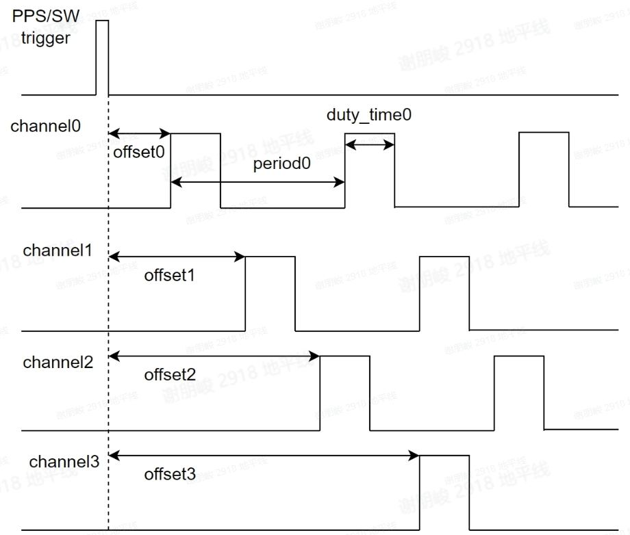
Formula calculations:
Period = 1000000 / fps
Offset = 1000000 - Period * fps
LPWM Triggering Methods
Software Trigger:
trigger_mode = 0, indicating internal software trigger. After configuring software trigger, the LPWM driver automatically provides a 1-second periodic software trigger based on hrtimer. Essentially, it writes to an LPWM register (LPWM_SW_TRIG) every second, causing LPWM to re-output square waves according to the configuration.Hardware Trigger:
trigger_mode = 1, indicating external trigger. Requires an external PPS (pulse per second) signal. Upon receiving the PPS signal, the hardware outputs square waves according to the software configuration. Every received PPS signal causes LPWM to re-output waves according to the configuration.External trigger requires configuration of
trigger_source. The external trigger source can be configured with the following values:
| Value of trigger_source | Corresponding Trigger Source | Description |
|---|---|---|
| 0-3 | pad_trigger_in | Hardware IO input PPS, currently not supported by software. |
| 4 | enet_ptp_pps | Reserved |
| 5 | sw_trigger_in | Software trigger |
| 6 | gps_trigger_in (TIME_SYNC2) | Hardware IO input PPS |
| 7 | mcu_trigger_in (TIME_SYNC1) | Hardware IO input PPS |
| 8 | time_sync2_in (TIME_SYNC3) | Hardware IO input PPS |
| 9 | time_sync3_in (TIME_SYNC4) | Hardware IO input PPS |
| 10 | camera_1sec_pulse_out | SIF module outputs PPS, directly connected internally to LPWM (recommended) |
LPWM Mapping Relationships
The mapping relationship between LPWM pin names and pad_trigger_in_x is as follows:
| LPWM0 | LSIO_SPI5_SCLK | pad_trigger_in_0 |
|---|---|---|
| LSIO_SPI5_SSN | pad_trigger_in_1 | |
| LSIO_SPI5_MISO | pad_trigger_in_2 | |
| LSIO_SPI5_MOSI | pad_trigger_in_3 | |
| LPWM1 | LSIO_SPI3_SCLK | pad_trigger_in_0 |
| LSIO_SPI3_SSN | pad_trigger_in_1 | |
| LSIO_SPI3_MISO | pad_trigger_in_2 | |
| LSIO_SPI3_MOSI | pad_trigger_in_3 |
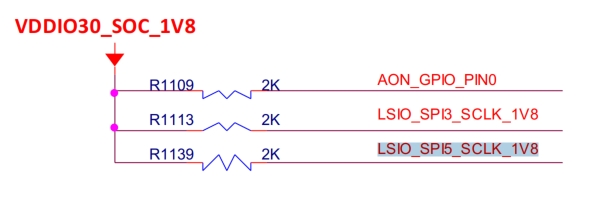
Referring to the EVB_X5 schematic, the LPWM trigger pin for the camera sensor on the MIPI0 interface is LSIO_SPI5_SCLK. As per the table above, this corresponds to LPWM0. The device tree association configuration is as follows:
&lpwm0 {
	status = "okay";
	/* conflict with camera pwd gpio */
	pinctrl-names = "default";
	pinctrl-0 = <&pinctrl_lpwm0_0 &pinctrl_lpwm0_1
			&pinctrl_lpwm0_2 &pinctrl_lpwm0_3>;
};

&vin_vcon0 {
	status = "okay";
	/* camera sensor
	 * reset gpio:	AON_GPIO0_00:	498
	 * pwd gpio:	LSIO_GPIO1_00:	347
	 */
	pinctrl-names = "default";
	pinctrl-0 = <&aon_gpio_0>;
	gpio_oth = <498>;   //reset gpio
	bus = <4>; //i2c4
	lpwm_chn = <0>;  //open lpwm0 - channel0
};
Key parameter explanations:
lpwm0: A reference node referring to the hardware module named lpwm0.pinctrl-0 (lpwm): This property specifies the specific pin control configuration (pinmux) associated with the lpwm0 device.pinctrl_lpwm0_0: Configuration node attribute, setting the pin to LSIO_SPI5_SCLK, with pin multiplexing attribute as Lite PWM0 output.
	pinctrl_lpwm0_0: pinctrl_lpwm0_0 {
  	horizon,pins = <
  		LSIO_SPI5_SCLK	LSIO_PINMUX_2	BIT_OFFSET8	 MUX_ALT2	&pconf_pwm_1v8
  	>;
  };
vin_con0: Video input control node named vin_vcon0.lpwm_chn: Selects which LPWM channel to enable. Channel 0 corresponds to the mapped pin LSIO_SPI5_SCLK for LPWM.
When the device tree vin_vcon0 controller is referenced, the trigger pin corresponding to LPWM channel 0 will output a square wave signal according to the parameters configured in the lpwm_attr structure.
Sysfs Node Debugging
When operating LPWM on the target board, use the cat command to read the device/uevent file under pwmchip to distinguish between PWM and LPWM nodes.
Check the LPWM controller node in x5.dtsi as follows:
lpwm0: lpwm@34100000 {
	compatible = "hobot,hobot-lpwm";
	status = "disabled";
	reg = <0x34100000 0x10000>;
	lpwm-int-status = <&lsio_sys_con 0x0>;
	interrupt-parent = <&gic>;
	interrupts = <GIC_SPI 91 IRQ_TYPE_LEVEL_HIGH>;
	clocks = <&hpsclks X5_LSIO_LPWM0_CLK>, <&hpsclks X5_LSIO_LPWM0_PCLK>;
	clock-names = "lpwm_sclk", "lpwm_pclk";
	#pwm-cells = <2>;
	resets = <&socrst LSIO_LPWM0_RESET>;
};
root@buildroot:~# cat /sys/class/pwm/pwmchip2/device/uevent
DRIVER=hobot-lpwm
OF_NAME=lpwm
OF_FULLNAME=/soc/a55_apb0/lpwm@34100000
OF_COMPATIBLE_0=hobot,hobot-lpwm
OF_COMPATIBLE_N=1
OF_ALIAS_0=lpwm0
MODALIAS=of:NlpwmT(null)Chobot,hobot-lpwm
It can be seen that pwmchip2’s address is 0x34100000 and the corresponding driver is hobot-lpwm. In the DTS, lpwm0’s address is 0x34100000, therefore lpwm0 corresponds to pwmchip2.
root@buildroot:/sys/class/pwm# cd pwmchip2
root@buildroot:/sys/class/pwm/pwmchip2# ls
device  export  npwm  power  subsystem  uevent  unexport
device: This is a symbolic link pointing to the actual hardware device node. Accessing this file allows the system to retrieve or modify attributes related to the device.
npwm: Indicates the number of channels contained in the current LPWM, usually 4.
export: Users can write the channel number to the export file to expose it to the
/sys/class/pwm/pwmchip2/pwmXdirectory (X is the LPWM channel number). For example,echo "0~3" > unexportderegisters a channel. Each channel can only be requested once; subsequent requests return BUSY.power: This file provides information related to device power management, including details such as whether power-saving mode is enabled or whether power is turned on.
subsystem: This directory is a symbolic link pointing to the subsystem to which the LPWM device belongs. Subsystems are part of Linux’s device management hierarchy, indicating the category to which the device belongs.
uevent: Used to manage udev (device manager) events, typically used to notify the system of device changes.
unexport: Allows users to write to cancel exporting an LPWM channel. If an LPWM channel has already been exported (via the export file), users can write the channel number to the unexport file to cancel the export, making the LPWM channel unavailable.
Use echo to set parameters such as period and duty_cycle. Note that the Linux LPWM framework parameter precision is 1ns; input values are rounded to the nearest 1μs before being set into registers. Therefore, period/duty_cycle input values need to be multiplied by 1000.
Request and register LPWM0 channel:
root@buildroot:/sys/class/pwm/pwmchip2# echo 0 > export
root@buildroot:/sys/class/pwm/pwmchip2# cd pwm0
Set period to 30Hz:
root@buildroot:/sys/class/pwm/pwmchip2/pwm0# echo 33333000 > period
Set duty cycle to 0.3%:
root@buildroot:/sys/class/pwm/pwmchip2/pwm0# echo 100000 > duty_cycle
Enable or disable LPWM output:
root@buildroot:/sys/class/pwm/pwmchip2/pwm0# echo 1 > enable
root@buildroot:/sys/class/pwm/pwmchip2/pwm0# echo 0 > enable
Hardware Debugging
Refer to the EVB X5 schematic. Using LPWM0 channel 0, the corresponding pin is LSIO_SPI5_SCLK as shown:
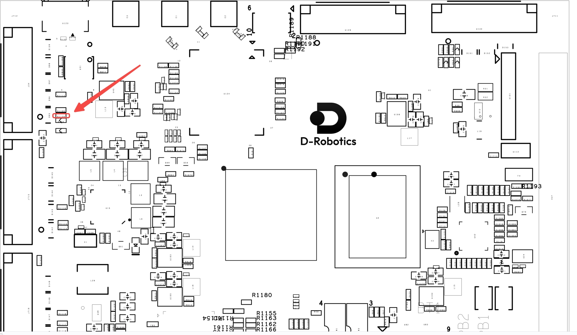
The corresponding development board pinout is as follows:
During sample execution, use an oscilloscope to probe as shown:
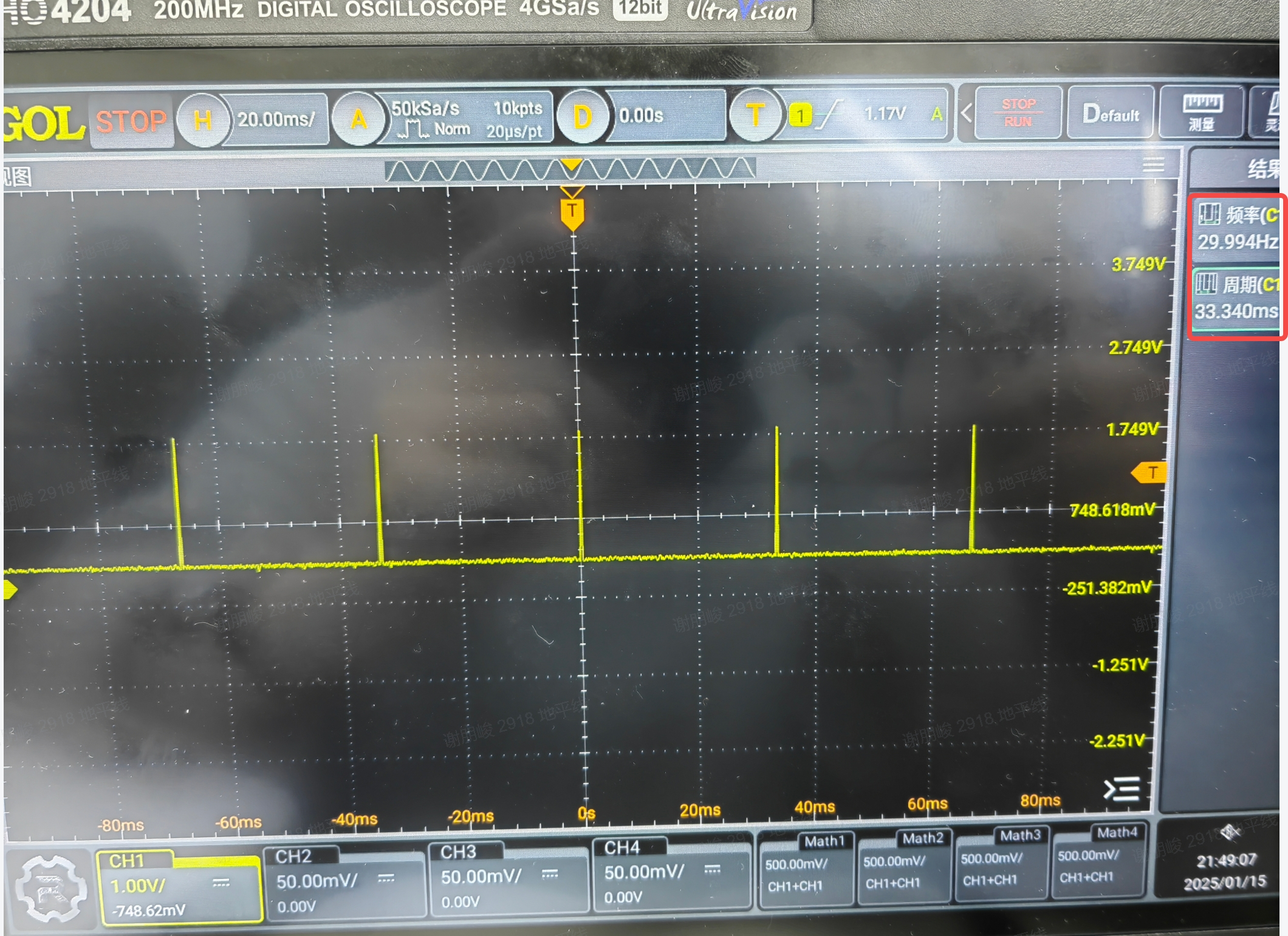
The frequency and period observed on the oscilloscope match the LPWM parameters in the configuration file.
4.3.10.6. Common Issues
Q: If the source trigger stops after some time, will LPWM continue to output square waves?
A: Yes, LPWM will continue to output square waves according to the configured period. However, the offset function becomes ineffective because without a trigger, the accuracy of subsequent LPWM square waves cannot be guaranteed, i.e., the period of the square wave may have errors.
Q: LPWM trigger and interrupt mechanism
A: The signal sent by LPWM to CIM is generated on every rising edge of the output waveform. LPWM interrupts, however, are generated based on the sync signal from the external trigger source.