4.3.17. LCD Driver Debug Guide
4.3.17.1. LCD Overview
LCD (Liquid Crystal Display) is one of the most common display devices in embedded systems. It renders images by using liquid crystal materials to change light transmission and polarization under an electric field. Since liquid crystals themselves do not emit light, LCDs typically require a backlight module to produce visible images; they also rely on high-speed display interfaces to transmit image data to the host SoC, and use a control channel for display parameter configuration and status management.
The X5 series boards provide a complete and highly integrated set of interfaces for LCD display, including MIPI DSI, I2C, reset signals, power input, and backlight control, enabling developers to easily and reliably connect various LCD panels and accelerate display function development and debugging.
4.3.17.2. Interface Description
The EVB board provides a 24-pin LCD interface, which mainly includes:
1 MIPI DSI clock lane
4 MIPI DSI data signals
1 I2C interface
GND, 3.3V power
RST reset pin
VLEDA, VLEDK backlight power/control pins
The X5 MD board provides a 22-pin LCD interface, which is similar in overall design to the EVB board, with the only difference being in the backlight power section: it does not include VLEDA and VLEDK backlight control pins.
4.3.17.3. Specifications
The MIPI-DSI interface specifications of X5 are as follows:
Supports up to four data lanes
Maximum rate per lane is
2.5GbpsSupports
Non-Burst-Sync-Pulsesynchronization pulse mode,Non-Burst-Sync-Eventsynchronization event mode, andBurstburst modeSupports
MIPI_DSI_CLOCK_NON_CONTINUOUSnon-continuous clock mode andMIPI_DSI_CLOCK_CONTINUOUScontinuous clock mode
4.3.17.4. Functional Principles
MIPI DSI
MIPI DSI (Display Serial Interface) is a high-speed serial communication standard between the host SoC and the LCD display module, responsible for sending initialization commands and transmitting video frame data. Its core consists of 1 clock Lane + multiple data Lanes, used for synchronization and data transmission respectively. DSI operation includes two main phases: Initialization Phase (Command Mode) and Video Data Transmission Phase (Video Mode).
Initialization Phase (Command Mode)
After the LCD is powered on, it first enters low-power LP mode. The host sends initialization commands to the LCD driver chip via MIPI DSI. This process is accomplished through DCS (Display Command Set) or vendor-specific commands. The initialization process generally includes the following steps:
Enter DSI LP mode
Perform hardware pin reset, or send a DSI software reset command
DCS Soft Reset (0x01)Send register configuration sequence
This step is the core of LCD initialization. Each LCD has its own register script, which includes:
Color format settings (e.g., RGB888, RGB565)
Lane count configuration (1/2/4 Lane)
Vertical/horizontal timing parameters (VBP/VFP/HBP/HFP)
Refresh rate and polarity settings
Gamma curve and power voltage parameters
Driver chip internal register initialization
Video Data Transmission Phase (Video Mode)
After initialization is complete, the LCD enters the display working state. At this point, DSI switches to HS (High-Speed) mode for continuous video frame transmission.
Working Characteristics
Uses high-speed differential signaling
Data rates can reach hundreds of MHz to several GHz
Continuously outputs full-frame RGB pixel data
Frame rates are typically 60Hz / 90Hz / 120Hz
Data Encapsulation Format
Pixel data is encapsulated as DSI Long Packets:
Video Line Packet
Each line of pixel data is encapsulated as a Long Packet, containing:
Packet Header (byte type, length, data ID)
e.g.: 0x39 (Long Write)
Payload: One full line of pixel data (RGB888/RGB565, etc.)
ECC/CRC checksum: Ensures data integrity
An entire frame consists of multiple line packets, combined with synchronization signals (VSync/HSync) to form a complete display image.
Touch
In most small and medium-sized LCD display modules, touch screens (mainly capacitive touch screens) typically communicate with the host SoC via the I2C interface. The touch IC is responsible for collecting touch coordinates, gestures, and other information, and reports it to the system in data packets via I2C. After parsing by the upper-layer input subsystem, it is converted into click, swipe, and other interaction events.
The most commonly used I2C capacitive touch screen controllers on embedded platforms include:
Goodix: GT911, GT5688, GT7388, etc.
FocalTech: FT5436, FT5x06, FT6336, etc.
Ilitek: ILI210x series
Himax: HX8526, HX83102, etc.
Mstar (merged into Novatek): MSG22xx series
These ICs all operate via the I2C interface with similar protocol styles, making system porting relatively easy. You can obtain drivers from the panel manufacturer or touch IC vendor.
Backlight Control
The X5 EVB uses LPWM 1_1 to output a PWM dimming signal. The SY7200AABC receives this signal and generates LED positive voltage (VLEDA) through its internal boost circuit, and produces LED negative current (VLEDK) through constant current control, thereby driving the LCD backlight and enabling brightness adjustment.
PWM control signal input (DIM/PWM pin)
The PWM duty cycle corresponds to the desired backlight brightness, for example:
High duty cycle -> large dimming command -> large LED current -> brighter backlight
Low duty cycle -> reduced brightness
0% duty cycle can turn off the backlight
SY7200AABC samples the PWM signal and converts it into an LED current adjustment value through internal dimming control
4.3.17.5. Debugging Procedure
Obtain Screen Information
Before adding a new display driver, the following information must be determined:
Display timing parameters:
hbp,hfp,hsa,vbp,vfp,vsaDisplay initialization sequence
Transmission mode supported by the display:
burstornon-burstClock mode supported by the display:
continuousornon-continuousDisplay lane count:
1,2, or4Touch screen driver
Backlight control method
Taking the JC050HD134 display as an example, the following information is obtained from the configuration provided by the manufacturer:
#define Width 720
#define Height 1280

#define VFP 20
#define VBP 20
#define VSA 4

#define HFP 32
#define HBP 20
#define HSA 20
Initialization sequence
DSI_CMD(0x04);DSI_PA(0xB9);
DSI_PA(0xF1);
DSI_PA(0x12);
DSI_PA(0x83);

DSI_CMD(0x1C);DSI_PA(0xBA);
DSI_PA(0x33); // 1
DSI_PA(0x81); // 2
DSI_PA(0x05); // 3
DSI_PA(0xF9); // 4
DSI_PA(0x0E); // 5
DSI_PA(0x0E); // 6
DSI_PA(0x20); // 7
DSI_PA(0x00); // 8
DSI_PA(0x00); // 9
DSI_PA(0x00); //10
DSI_PA(0x00); //11
DSI_PA(0x00); //12
DSI_PA(0x00); //13
DSI_PA(0x00); //14
DSI_PA(0x44); //15
DSI_PA(0x25); //16
DSI_PA(0x00); //17
DSI_PA(0x91); //18
DSI_PA(0x0A); //19
DSI_PA(0x00); //20
DSI_PA(0x00); //21
DSI_PA(0x02); //22
DSI_PA(0x4F); //23
DSI_PA(0xD1); //24
DSI_PA(0x00); //25
DSI_PA(0x00); //26
DSI_PA(0x37); //27
Transmission mode supported by the display:
non-burstClock mode supported by the display:
continuousDisplay lane count:
4Touch screen driver:
NoneBacklight control method:
Adapted for 24-pin VLEDA, VLEDK
Kernel Driver Level
There is a well-debugged reference code in the kernel: panel-atk-md0550.c. Subsequent display drivers can be derived from this driver.
Copy kernel/drivers/gpu/drm/panel/panel-atk-md0550.c and rename it to panel-jc-050hd134.c.
All the following modifications are based on panel-jc-050hd134.c.
Modify the name field in the panel_simple_dsi_driver structure to panel-jc-050hd134:
static struct mipi_dsi_driver panel_simple_dsi_driver = {
	.driver =
		{
			.name		= "panel-jc-050hd134",
			.of_match_table = dsi_of_match,
		},
	.probe	  = panel_simple_dsi_probe,
	.remove	  = panel_simple_dsi_remove,
	.shutdown = panel_simple_dsi_shutdown,
};
Modify the drm_display_mode structure:
static const struct drm_display_mode jc_050hd134_mode { // Rename structure to jc_050hd134_mode
	.clock	     = 65000, // Pixel clock in kHz, calculated as: fps * (htotal + vtotal)
	.hdisplay    = 720, // Horizontal active area width
	.hsync_start = 720 + 32, // hdisplay + hfp
	.hsync_end   = 720 + 32 + 20, // hsync_start + hsa
	.htotal	     = 720 + 32 + 20 + 20, // hsync_end + hbp
	.vdisplay    = 1280, // Vertical active area height
	.vsync_start = 1280 + 20, // vdisplay + vfp
	.vsync_end   = 1280 + 20 + 4, // vsync_start + vsa
	.vtotal	     = 1280 + 20 + 4 + 20, // vsync_end + vbp
	.flags	     = DRM_MODE_FLAG_NHSYNC | DRM_MODE_FLAG_NVSYNC, // Polarity
};
Modify the panel_desc_dsi structure:
static const struct panel_desc_dsi jc_050hd134 { // Rename structure to jc_050hd134
	.desc =
		{
			.modes	   = &jc_050hd134_mode, // Point to timing structure
			.num_modes = 1, // Number of timing modes for this panel, usually one
			.bpc	   = 8, // Bits per color component? RGB888 means 8 bits per color, RGB666 means 6 bits per color
			.size = // Physical size of active area in mm (millimeters)
				{
					.width	= 62,
					.height = 110,
				},
			.connector_type = DRM_MODE_CONNECTOR_DSI,
		},
	.flags	= MIPI_DSI_MODE_VIDEO | MIPI_DSI_MODE_VIDEO_SYNC_PULSE, // DSI mode flags, indicating the panel operates in video mode and non-burst mode
    // For more flags, refer to kernel/include/drm/drm_mipi_dsi.h
	.format = MIPI_DSI_FMT_RGB888, // Panel color format
	.lanes	= 4, // Number of data lanes
};
mode_flags are used to describe the data transmission method and link behavior between the DSI host and the display panel, as detailed below:
| mode_flags | Description |
|---|---|
| MIPI_DSI_MODE_VIDEO | Enable video mode, the host continuously sends pixel data according to display timing. |
| MIPI_DSI_MODE_VIDEO_BURST | Enable Burst video mode, pixel data is sent in burst fashion. |
| MIPI_DSI_MODE_VIDEO_SYNC_PULSE | Enable synchronization pulse mode, HSYNC/VSYNC are sent as independent pulses. The timing is closer to the traditional RGB interface with the best compatibility, and is the recommended configuration for most LCDs. |
| MIPI_DSI_MODE_VIDEO_AUTO_VERT | Enable automatic vertical count mode, the DSI controller automatically manages vertical line counting. |
| MIPI_DSI_MODE_VIDEO_HSE | Send HSYNC End packets during VSYNC pulses and vertical porch regions. Used for some panels with strict timing requirements. |
| MIPI_DSI_MODE_VIDEO_NO_HFP | Disable horizontal front porch. |
| MIPI_DSI_MODE_VIDEO_NO_HBP | Disable horizontal back porch. |
| MIPI_DSI_MODE_VIDEO_NO_HSA | Disable horizontal sync active region. |
| MIPI_DSI_MODE_VSYNC_FLUSH | Flush display FIFO during VSYNC pulses to prevent residual old data. |
| MIPI_DSI_MODE_NO_EOT_PACKET | Disable EoT (End of Transmission) packets in HS mode. Some panels or PHYs have incomplete EoT packet support; disabling can improve stability. |
| MIPI_DSI_CLOCK_NON_CONTINUOUS | Enable non-continuous clock mode. The DSI Clock Lane can enter LP state during idle periods, reducing power consumption. |
| MIPI_DSI_MODE_LPM | Enable Low Power Mode (LP) for data transmission. This is critical; most panel initialization commands (DCS/Generic Command) must be sent in LP mode. |
| MIPI_DSI_HS_PKT_END_ALIGNED | In high-speed mode (HS), whether the end times of data packets on multiple Data Lanes are aligned. |
Among them, MIPI_DSI_MODE_VIDEO, MIPI_DSI_MODE_VIDEO_SYNC_PULSE, and MIPI_DSI_MODE_LPM are the most commonly used flags in practical projects and are often required configurations.
Modify dsi_of_match for device tree binding preparation:
static const struct of_device_id dsi_of_match[] = {
	{.compatible = "jc-050hd134", .data = &jc_050hd134},
	{
		/* sentinel */
	}};
MODULE_DEVICE_TABLE(of, dsi_of_match);
Modify the panel_simple_dsi_init function, which actually calls dsi_dcs_write_seq to write the mipi initialization sequence into the panel.
If the initialization parameters you receive from the display vendor are in the following format:
DSI_CMD(0x04);DSI_PA(0xB9);
DSI_PA(0xF1);
DSI_PA(0x12);
DSI_PA(0x83);

DSI_CMD(0x1C);DSI_PA(0xBA);
DSI_PA(0x33); // 1
DSI_PA(0x81); // 2
DSI_PA(0x05); // 3
DSI_PA(0xF9); // 4
DSI_PA(0x0E); // 5
DSI_PA(0x0E); // 6
DSI_PA(0x20); // 7
DSI_PA(0x00); // 8
DSI_PA(0x00); // 9
DSI_PA(0x00); //10
DSI_PA(0x00); //11
DSI_PA(0x00); //12
DSI_PA(0x00); //13
DSI_PA(0x44); //14
DSI_PA(0x25); //15
DSI_PA(0x00); //16
DSI_PA(0x91); //17
DSI_PA(0x0A); //18
DSI_PA(0x00); //19
DSI_PA(0x00); //20
DSI_PA(0x02); //21
DSI_PA(0x4F); //22
DSI_PA(0xD1); //23
DSI_PA(0x00); //24
DSI_PA(0x00); //25
DSI_PA(0x37); //26

......
Convert to driver code:
dsi_dcs_write_seq(dsi, 0xb9, 0xF1, 0x12, 0x83);
dsi_dcs_write_seq(dsi, 0xBA, 0x33, 0x81, 0x05, 0xF9, 0x0E, 0x0E, 0x20, 0x00, 0x00, 0x00,
			  0x00, 0x00, 0x00, 0x00, 0x44, 0x25, 0x00, 0x91, 0x0A, 0x00, 0x00, 0x02,
			  0x4F, 0xD1, 0x00, 0x00, 0x37);
......
Note that the first value in each vendor-provided initialization sequence indicates the length of that sequence and should not be included when converting to driver code, as it will be automatically calculated during write operations.
If the initialization sequence from the vendor is in the following format:
panel-init-sequence-zero = [
 39 00 04 B9 FF 83 94
 15 00 02 36 01
 39 00 07 BA 63 03 68 6B B2 C0
 39 00 0B B1 48 12 72 09 32 54 71 71 57 47
......
]
Convert to driver code:
	dsi_dcs_write_seq(dsi, 0xb9, 0xff, 0x83, 0x94);
	dsi_dcs_write_seq(dsi, 0x36, 0x01);
	dsi_dcs_write_seq(dsi, 0xba, 0x63, 0x03, 0x68, 0x6b, 0xb2, 0xc0);
	dsi_dcs_write_seq(dsi, 0xb1, 0x48, 0x12, 0x72, 0x09, 0x32, 0x54, 0x71, 0x71, 0x57, 0x47);
Take the first sequence 39 00 04 B9 FF 83 94 as an example for explanation:
39 indicates that this initialization sequence uses
MIPI_DSI_DCS_LONG_WRITE(0x39) data type, which does not need to be written in driver code and will be automatically generated based on the parameter length
00 means delay 0ms after this write operation, which can be implemented viamsleep(ms)
04 indicates the length of the current write sequence, which will be automatically generated and does not need to be filled in
The following bytes are the actual initialization sequence
For displays requiring specific power-on and reset timing sequences, modify the gpio behaviors in the panel_simple_prepare and panel_simple_unprepare functions, which correspond to initialization and deinitialization states respectively.
Modify kernel/drivers/gpu/drm/panel/Kconfig and kernel/drivers/gpu/drm/panel/Makefile
Kconfig:
config DRM_PANEL_JC_050HD134
	tristate "JC 050HD134 panel"
	depends on OF
	depends on DRM_MIPI_DSI
	depends on BACKLIGHT_CLASS_DEVICE
	select VIDEOMODE_HELPERS
	help
	  Say Y here if you want to enable support for the JC050HD134
	  panel with 720x1280 resolution. This panel supports
	  MIPI DSI interface.
Makefile:
obj-$(CONFIG_DRM_PANEL_JC_050HD134) += panel-jc-050hd134.o
Kernel Device Tree Level
In the board-level device tree, using kernel/arch/arm64/boot/dts/hobot/x5-evb.dtsi as an example:
Add the following properties to the mipi_dsi0 node:
&mipi_dsi0 {

	status = "okay";
	ports {
		port@1 {
			reg = <1>;
			mipi_dsi_out: endpoint {
				remote-endpoint = <&panel_in>;
			};
		};
	};

	dsi_panel0@0 {
		compatible = "jc-050hd134"; // Must match dsi_of_match
		reg = <0>;

		pinctrl-names = "default";
		pinctrl-0 = <&lsio_gpio0_14>; // Related to reset pin
		reset-gpios = <&ls_gpio0_porta 14 GPIO_ACTIVE_HIGH>; // Reset pin, active level depends on your display
		backlight = <&dsi_backlight>; // Backlight related

		port {
			panel_in: endpoint {
				remote-endpoint =
					<&mipi_dsi_out>;
			};
		};
	};

};
Add the dsi_backlight node:
&dsi_backlight {
	status = "okay";
	pwms = <&lpwm1 1 1000000>; // Hardware PCB dependent, check where your backlight PWM signal comes from; here indicates it comes from LPWM1_1
    // For other properties and information, refer to kernel/Documentation/devicetree/bindings/leds/backlight/pwm-backlight.yaml
};
Compilation
Please first refer to Chapter 4.1 to set up the compilation environment and ensure you can successfully compile an image before proceeding!
Run ./bd.sh boot menuconfig to enter the kernel configuration menu, then navigate to the Panels compilation option via the following path:
Device Drivers  --->
    Graphics support  --->
        Display Panels  --->
Locate JC 050HD134 panel, press space to compile it as a module, then save and exit.
Run ./bd.sh all to compile and generate the image, then flash the image onto the board, connect the display, and power on.
Testing
After successfully entering the kernel, execute the following commands to load the driver:
modprobe panel-jc-050hd134
modprobe vio_n2d
modprobe vs-x5-syscon-bridge
modprobe vs_drm
Then, run the dmesg command and check the end of the log for output similar to:
[ 3343.383052] vs-disp-sif 3e080000.vs-sif: Adding to iommu group 3
[ 3343.384118] vs-dc 3e000000.dc8000Nano: Adding to iommu group 4
[ 3343.385252] vs-bt1120 3e010000.bt1120: Adding to iommu group 5
[ 3343.387555] horizon-lsio-pinctrl 34180000.lsio_iomuxc: set pin = 14 direction to input
[ 3343.387567] horizon-lsio-pinctrl 34180000.lsio_iomuxc: map pin14 to gpio[0] - 14
[ 3343.387635] panel-jc-050hd134 3e060000.mipi_dsi0.0: supply power not found, using dummy regulator
[ 3343.391241] vs-drm 3e000000.disp_apb:display-subsystem: bound 3e080000.vs-sif (ops sif_component_ops [vs_drm])
[ 3343.391529] vs-drm 3e000000.disp_apb:display-subsystem: bound 3e000000.dc8000Nano (ops dc_component_ops [vs_drm])
[ 3343.391692] vs-drm 3e000000.disp_apb:display-subsystem: bound 3e010000.bt1120 (ops bt1120_component_ops [vs_drm])
[ 3343.391730] vs-drm 3e000000.disp_apb:display-subsystem: bound 3e000000.disp_apb:bt1120_bridge (ops bt1120_bridge_component_ops [vs_drm])
[ 3343.391764] vs-drm 3e000000.disp_apb:display-subsystem: bound 3e000000.disp_apb:bt1120_bridge_wb (ops bt1120_bridge_component_ops [vs_drm])
[ 3343.391816] vs-drm 3e000000.disp_apb:display-subsystem: bound 3e060000.mipi_dsi0 (ops dsi_component_ops [vs_drm])
[ 3343.391917] vs-drm 3e000000.disp_apb:display-subsystem: bound 3e000000.disp_apb:dsi-encoder (ops encoder_component_ops [vs_drm])
[ 3343.391976] vs-drm 3e000000.disp_apb:display-subsystem: bound 3e000000.disp_apb:hdmi-encoder (ops encoder_component_ops [vs_drm])
[ 3343.392815] [drm] Initialized vs-drm 1.0.0 20191101 for 3e000000.disp_apb:display-subsystem on minor 0
When the line [drm] Initialized vs-drm 1.0.0 20191101 for 3e000000.disp_apb:display-subsystem on minor 0 appears, it indicates that the display driver has loaded successfully.
Run modetest -M vs-drm -c to check the status of connectors:
Connectors:
id      encoder status          name            size (mm)       modes   encoders
73      0       connected 		DSI-1           62x110             1       72
  modes:
        index name refresh (Hz) hdisp hss hse htot vdisp vss vse vtot
  #0 720x1280 61.99 720 752 772 792 1280 1300 1304 1324 65000 flags: nhsync, nvsync; type: preferred, driver
  props:
        1 EDID:
                flags: immutable blob
                blobs:

                value:
        2 DPMS:
                flags: enum
                enums: On=0 Standby=1 Suspend=2 Off=3
                value: 0
        5 link-status:
                flags: enum
                enums: Good=0 Bad=1
                value: 0
        6 non-desktop:
                flags: immutable range
                values: 0 1
                value: 0
        4 TILE:
                flags: immutable blob
                blobs:

                value:
Test using the command: modetest -M vs-drm -a -s 73@31:720x1280 -P 33@31:720x1280@NV12
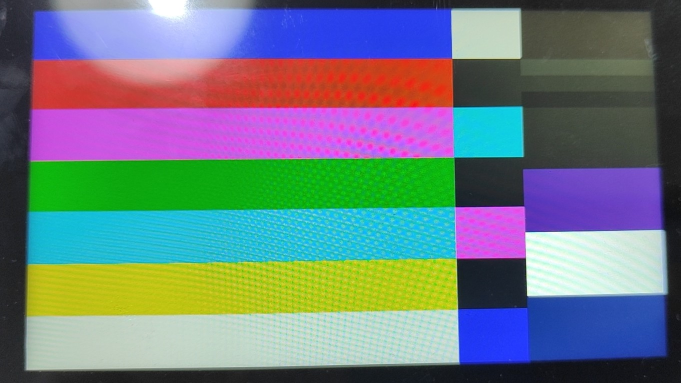
If everything goes smoothly, the connected display will light up and show the pattern shown in the image below (image rotated):