1. Preface
1.1. Overview
This document serves as the user manual for the X5 chip solution, providing developers with usage instructions and development guidelines on various aspects including development environment setup, solution evaluation, software feature development, etc. The content covers development board usage, hardware design, system customization, application development, algorithm toolchain, and more.
1.2. General Description of the Delivery Package
The SDK delivery package mainly consists of several components: BSP source code, supporting documentation, hardware reference designs, sample examples, algorithm toolchain, and host-side tools. The modules in the release package are described as follows:
.
├── datasheet_and_design_guide                   # Chip datasheet, hardware reference design, including schematic, PCB, and BOM
│   ├── Datasheet                                # Chip datasheet
│   ├── HardwareDevelopmentGuide                 # Hardware reference design, including schematic, PCB, and BOM
│   ├── HardwareInterface                        # Development board hardware interface description
│   ├── Pinlist                                  # Chip IO configuration table, describing all IO pins' multiplexing, voltage domains, pull-up/down, etc. in tabular form
│   ├── RegisterManual                           # Chip register manual
│   └── TypicalScenarioPowerConsumption          # Typical power consumption estimation table under various workloads
└── X5_LNX_SDK                                   # Software SDK, including BSP, algorithm toolchain, user manuals, etc.
    └── LNX6.1.83_PL5.1_V1.0.14                  # SDK version number
        ├── ai_toolchain_package                 # Algorithm toolchain, including model conversion tools, etc.
        ├── board_support_package                # Board Support Package (BSP)
        │   ├── firmwares                        # Pre-built firmware images for development board flashing
        │   └── platform_source_code.tar.gz      # BSP source code
        ├── release_note_and_change_log          # Release notes and important change logs for the current version
        ├── software_tools                       # Host-side tools used during development, including flashing tools, driver software, ISP debugging tools, GDC debugging tools, etc.
        └── user_manual                          # User manuals, developer guides, software API manuals, algorithm toolchain user guides, FAQs, etc.
1.2.1. How to Access the Delivery Package
Users of the X5 chip can login in to the SDK Release System (contact your FAE to set up an account) to view released SDK delivery packages and learn how to download materials. If you encounter any technical issues during use, feel free to contact your FAE or our technical support team for assistance.
1.3. Chip Specifications
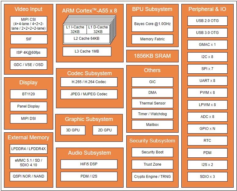
1.3.1. Chip Functional Block Diagram
1.3.2. System Software Architecture
1.3.3. Key Features
CPU:
Octa-core ARM Cortex-A55, 32 KB/32 KB L1 I/D, 64 KB L2, 1 MB L3 cache.
Typical operating frequency: 1.5 GHz.
BPU:
Bayesian architecture BPU, delivering up to 10 TOPS computing power.
Typical operating frequency: 1.0 GHz.
External Memory:
DDR
Supports x32 LPDDR4/LPDDR4X external DRAM.
Supports up to 8 GB memory capacity.
eMMC 5.1 Controller
Supports up to HS200 mode
Supports up to 8-bit data width
ISP:
Maximum processing capability: 3840x2160@60fps
Supports 3DNR
Supports 3A (AE/AWB/AF), supports third-party 3A algorithms
Video Input Interface:
Supports MIPI CSI video input:
4 MIPI CSI Rx ports
Each data lane up to 2.5 Gbps
Video input up to 5472 x 3076 @ 30fps
Supports RAW 8/10/12/14/16-bit formats and 8/10-bit YUV 422 format
Video Output Interface:
Supports BT1120 video output
Supports MIPI DSI video output
Supports Display Engine for layer composition
Video/Image Processing Units:
Video Scaling Engine (VSE):
Supports 1 channel of video upscaling
Supports 5 channels of video downscaling
Supports frame rate control
Supports OSD overlay
Video Codec:
Supports H.265 (HEVC) encoding and decoding:
Main profile @ L5.1
Supports H.264 (AVC) encoding and decoding:
Baseline/Constrained Baseline/Main/High profiles @ L5.2
H.264 supports SVC-T encoding
H.265/H.264 codec performance:
Maximum support: 3840 x 2160@60fps encoding
Maximum support: 3840 x 2160@60fps decoding
When encoder and decoder run simultaneously, supports 3840 x 2160@30fps encoding and decoding respectively
Supports JPEG encoding and decoding:
Supports JPEG baseline/extended
Supports simultaneous encoding and decoding at 3840 x 2160@30fps
Maximum supported resolution: 32768 x 32768 pixels
Minimum supported resolution: 16 x 16 pixels
Peripheral Interfaces:
1 x USB 3.0 (Dual-Role Device)
1 x USB 2.0 (Dual-Role Device)
1 x 1G Ethernet MAC
2 x SDIO
1 x QSPI
7 x SPI
8 x I2C
8 x UART
8 x PWM
8 x LPWM
8 x ADC
129 x GPIO
Timer
Watchdog
Mailbox
Chip Physical Specifications:
TSMC 12nm FinFET Compact (FFC) process technology
FCCSP563 package, 0.65 mm pin pitch, package size: 16 mm x 16 mm
1.4. Document Usage Guide
1.4.1. Chapter Introduction
This user manual provides a comprehensive guide for the development and application of the X5 chip, aiming to help users better understand and utilize the chip’s features and capabilities. Below is a brief introduction to each chapter, helping users quickly grasp the document structure and content for more efficient development, learning, and work.
1. Preface:
This section introduces the purpose and scope of the manual, providing basic background information about the chip, including its intended applications, target user groups, and recommendations for using this manual.
2. Quick Start:
This section introduces fundamental concepts and commonly used functions of the chip, offering a quick start guide to help users get started with the development board quickly. It includes environment configuration, software installation, firmware flashing, and other basic operations. This part also provides detailed descriptions of the development board’s hardware interfaces and their basic usage.
3. Sample Code Usage Guide:
This section provides a series of sample codes aimed at accelerating user development. Each sample code covers a specific function or application scenario, accompanied by detailed explanations and usage examples.
4. BSP Development Guide:
This is one of the core sections, detailing how to perform low-level chip development, including setting up the development environment, compilation instructions, hardware bring-up guidance, driver development guide, system component development, driver functional unit testing, commonly used command usage, and system debugging methods. Through this content, users can gain deep insights into the internal architecture and working principles of the chip, enabling effective low-level driver and system software development.
5. Multimedia Development Guide:
This section introduces the chip’s multimedia functions, interface descriptions, and basic development workflows, covering development content and API interfaces for video processing, image processing, GPU, DSP, and other functional modules.
6. Quantization Toolchain Development Guide:
This section explains how to use the quantization toolchain for development, covering model quantization and conversion, model training, optimization, and deployment, aiming to help users leverage machine learning and AI technologies for application development.
7. FAQ:
This section lists frequently asked questions and answers, aiming to help users resolve various issues they may encounter during development. Content ranges from basic operations to advanced development techniques, providing comprehensive support and guidance.
8. Suggestions and Feedback:
This section provides channels for user feedback and suggestions, allowing users to participate in the optimization of the system or documentation through feedback.
1.4.2. Reading Recommendations
Chapters 1, 2, and 3 introduce development board interfaces, flashing methods, and usage of various application examples. New users of this SDK are recommended to read these chapters to fully understand basic operations and functional applications. These chapters are especially helpful for completing functional evaluations.
Chapters 4, 5, 6, and 7 cover BSP, multimedia, and algorithm toolchain development. During the project development phase, you should thoroughly read these chapters to understand development methodologies, interface definitions, and common troubleshooting information.