X5 eFuse 介绍
以下
概述
eFuse(电子
eFuse 通常
X5 eFuse 特性
X5 eFuse 分为 secure bank 和 non-secure bank,每个 region 有 32 个 bank,每个 bank 是 32bit,即
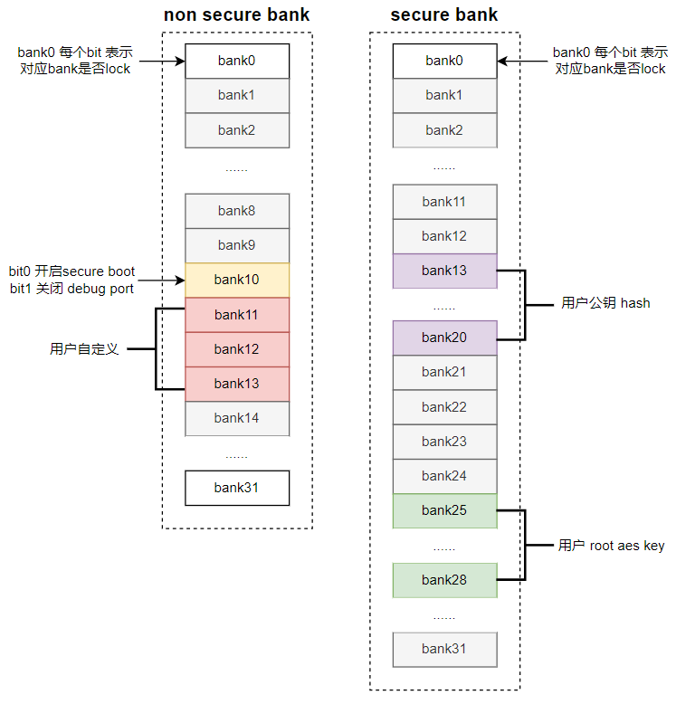
支持
eFuse 比特
位 默认 均 为 0,可以 从 0 写为 1 ,但 不能 从 1 写为 0 (eFuse 硬件 特性) 用户
可 烧写 的 区域
| 区域 | bank | 用途 | 备注 |
|---|---|---|---|
| secure | 13 - 20 | 公钥hash 对应bl2_rot_prikey.pem |
当 |
| secure | 25 - 28 | 用户 |
|
| non-secure | 10 | 配置 |
当 |
| non-secure | 11 - 13 | 用户 |
在 |
特殊 bank 说明
secure 和 non-secure region 的 bank0 的
每个 bit 表示 对应 的 bank 是否 被 lock, 1 表示 lock, 0 表示 没有 lock. non-secure bank10 用于
设置 secure boot 和 JTAG 使能 开关,其 定义 如下
| 比特 |
功能 |
定义 | 默认值 |
|---|---|---|---|
| bit0 | enable secure boot | 0 : 关闭 secure boot 1 : 开启 secure boot | 0 |
| bit1 | disable debug port | 0 : 开启 JTAG 1 : 关闭 JTAG | 0 |
eFuse 的
BL2 烧录 eFuse
eFuse 配置文件
eFuse 的device/horizon/x5/board_cfg/soc/bl2_cfg/bl2_cfg.json。
其
{
    "bl2_cfg": {
        ...
      },
      "efuse_cfg": {
        "bypass": 1,
        "secure_boot": "false",
        "debug_disable": "false",
        "burn_user_rot_key": "false",
        ...
      },
	   "nonsecure_bank": {
            "bank11":["0x0"],
            "bank12":["0x0"],
            "bank13":["0x0"]
        },
}
参数
bypass: bl2 是否烧录 eFuse 1 : 表示 bypass
0 : 表示 bl2 将
烧录 eFuse
secure_boot: 是否开启 secure boot,对应 eFuse 的 non-secure bank10 bit0 false : 表示
不 开启 secure boot true : 表示
开启 secure boot,开启 会 将 Uboot 公钥 的 hash 烧写 到 eFuse secure region bank13~20
debug_disable: 是否禁止 debug port,对应 eFuse 的 non-secure bank10 bit1 false : 表示
开启 debug port true : 表示
禁止 debug port
burn_user_rot_key: 是否要 烧写 user root aes key。对应 的 key 文件 位于 device/horizon/x5/board_cfg/soc/bl2_cfg/user_root.key,同时注意 为小端 格式 nonsecure_bank: 要烧写 的 non-secure bank11/12/13 的 值
注意:
在
烧写 eFuse 之后,相应 的 bank 都 会 被 lock BL2 CFG 会
被 打包 到 镜像 中,如果 要 烧录 user root aes key,直接 将 key 保存 到 外部 storage,如 eMMC 中 并 不 安全,推荐 使用 以下 方法: 在 Linux 下
调用 接口 的 形式 更新 key 通过 UART/USB 形式
下载 miniboot 更新 key,路径 位于 out/product/uart_usb,并妥善 保存 该 文件夹。
eFuse 电源控制与烧录状态
eFuse 烧录状态
BL2 可以
以 device/horizon/x5/board_cfg/soc/bl2_cfg/bl2_cfg.json 为例,通过 efuse_cfg 配置 :
{
    "bl2_cfg": {
        ...
      },
      "efuse_cfg": {
        "bypass": 1,
        "secure_boot": "false",
        "debug_disable": "false",
        "burn_user_rot_key": "false",
        "status_gpio" : {
            "gpio_sub": "none",
            "gpio_group": 0,
            "gpio_num": 0
        },
        "delay_before_efuse": 0,
        "delay_after_efuse": 0
      },
        ...
}
status_gpio字段 表示 用于 指示 eFuse 烧写 状态 的 GPIO 信息,其 可 配置 参数 如下 gpio_sub: 表示 GPIO 所在的 subsystem,包括 aon,hsio,lsio,dspgpio_group: 表示 GPIO 的 groupgpio_num: 表示 GPIO 号polarity:可选 参数,表示 GPIO 的 默认值, default_low 默认 为 低, default_high 默认 为 高,该字 段 不 写 时,选择 为 default_low
delay_before_efuse: 烧写前 操作 power_gpio后到 真正 烧写 eFuse 的 延迟时间,单位 ms,目的 是 为了 保证 在 烧写 之前 eFuse 电源 是 稳定 的 默认
配置 为 0 时,延迟时间 为 1s 这个
时间 只有 在 真正 烧写 eFuse 时才 会 起 作用。例如 在 产线 烧录 固件 后 第一次 启动, BL2 将要 烧录 eFuse,此时 延时 时间 起 作用,之后 再次 启动 由于 不会 重复 烧写 eFuse,因此 这个 延时 时间 也 就 失效 了
delay_after_efuse: 表示烧写 完成 之后 的 动作,其 定义 如下
| delay_after_efuse | 烧写 |
|---|---|
| 0 | 烧写 |
| -1 | 烧写 |
| 正值 | 烧写 |
| 负值(不 |
烧写 |
eFuse 电源控制
在
注意: X5 默认aon gpio0_7 控制 eFuse 电源,如果power_gpio 描述
如下status_gpio 字
{
    "bl2_cfg": {
        ...
      },
      "efuse_cfg": {
        ...
        "power_gpio" : {
            "gpio_sub": "none",
            "gpio_group": 0,
            "gpio_num": 0
        },
        ...
      },
        ...
}
使用示例
示例 : 以 aon gpio0_7 为 power GPIO,hsio1_1 为 state GPIO ,两个 GPIO 默认值
| power GPIO | status | 描述 |
|---|---|---|
| 先 |
拉高 | 烧写 |
| 先 |
拉低 | 烧写 |
| 一直 |
x | 未 |
uboot 读写 eFuse
在 uboot 命令
读取 eFuse
uboot 读取 eFuse 信息efuse dump
该
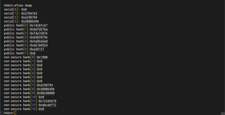
读取 eFuse 指定 bank 值
uboot 读取 eFuse 指定 bank 值efuse read [type] [bank_index]
参数
type: secure 表示是 读取 secure region, nonsecure 表示 读取 non-secure region bank_index: 表示要 读取 的 bank 的 index, 16 进制 形式
注意: 可
secure region 的 bank0 , bank13~bank20 可以
读 non secure region 的
所有 bank 均 可 读
执行命令
Hobot>efuse read nonsecure 0xc
value:0xabcdef12
lock:true

Hobot>efuse read secure 0x13
value:0xed3137
lock:true
写入 eFuse
该
efuse write [type] [bank_index] [bank_value] [lock_status]
type: secure 表示写 secure region, nonsecure 表示 写 non-secure region bank_index: 表示要 写 的 bank 的 index, 16 进制 形式 bank_value: 表示要 写 的 bank 的 value, 16 进制 形式 lock_status: 烧写之后 是否 要 lock, 取值 范围 lock/unlock
注意: 可
secure region 的 bank13~bank20 , bank25~bank28 可
写 non-secure region 的 bank10/11/12/13 可
写。
示例: 将 0x1eff5f0d 写入 secure region bank20
Hobot>efuse write secure 0x14 0x1eff5f0d lock
write SECURE bank:0x14 success
注意事项
执行 efuse write 命令
之后,需要 在 重启 之后 才能 读 到 正确 的 数据 eFuse 电源
默认 是 关闭 状态,通过 aon gpio0_7来控制,在 efuse write 命令 中,其 控制 时序 如下 : 先
将 该 aon gpio0_7拉高,给 eFuse 上电等待 1S,待 eFuse 电源
稳定 之后,再 写 eFuse 写 eFuse 完成,控制 GPIO 下电
示例: 将 user root aes key 写入 secure bank 25 - 28
烧录 user root aes key,对应device/horizon/x5/board_cfg/soc/bl2_cfg/user_root.key,同时
$ hexdump user_root.key -C
00000000  78 56 34 12 89 67 45 23  9a 78 56 34 ab 89 67 45  |xV4..gE#.xV4..gE|
00000010
user root aes key 的
secure bank[25]=0x12345678

secure bank[26]=0x23456789

secure bank[27]=0x3456789a

secure bank[28]=0x456789ab
Linux 读写 eFuse
在 Linux 中libefuse.so,头文件drobot_efuse.h
API 参考
drobot_efuse_read : 读 eFuse 接口
drobot_efuse_write : 写 eFuse 接口
数据结构
efuse_type
enum efuse_type 表示 efuse 的
| 名称 | 含义 |
|---|---|
| EFUSE_SECURE | secure region |
| EFUSE_NONSECURE | non-secure region |
efuse_info
struct efuse_info 是
| 名称 | 类型 | 最小值 | 最大值 | 默认值 | 含义 |
|---|---|---|---|---|---|
| type | efuse_type | - | - | - | efuse 的 |
| bank | uint32_t | - | - | - | bank 的 index 值 |
| value | uint32_t | - | - | - | bank 的 value 值 |
| lock | bool | - | - | - | 该 bank 是否 lock |
接口说明
drobot_efuse_read
【函数声明】
int drobot_efuse_read(struct efuse_info *efuse);
【功能描述】
用于
【参数描述】
[IN] struct efuse_info *efuse : 要
读取 的 efuse bank 属性 结构 体 指针, efuse bank 属性 结构 体为 efuse_info
【返回值】
成功,返回 0
失败:异常
为 负值
drobot_efuse_write
【函数声明】
int drobot_efuse_write(struct efuse_info *efuse);
【功能描述】
用于
【参数描述】
[IN] struct efuse_info *efuse : 要
写入 的 efuse bank 属性 结构 体 指针, efuse bank 属性 结构 体为 efuse_info
【返回值】
成功,返回 0
失败:异常
为 负值
示例: 将 user root aes key 写入 secure bank 25 - 28
烧录 user root aes key,对应device/horizon/x5/board_cfg/soc/bl2_cfg/user_root.key,同时
$ hexdump user_root.key -C
00000000  78 56 34 12 89 67 45 23  9a 78 56 34 ab 89 67 45  |xV4..gE#.xV4..gE|
00000010
user root aes key 的
secure bank[25]=0x12345678

secure bank[26]=0x23456789

secure bank[27]=0x3456789a

secure bank[28]=0x456789ab
注意事项
开启 secure boot 的操作顺序
以下
non secure bank10 的 bit0 用于
公钥
的 hash 数据 保存 在 BSP 路径 out/deploy/uboot/pubkey-hash.txt,可以在 uboot 阶段 烧入 secure region bank13~20 。
强制开启 debug port
non secure bank10 的 bit1 用于
注意: 最
通过
以下 命令 获取 socid
hrut_socuid
将 socid 填充
到 BL2 CFG 文件 中
{
    "bl2_cfg": {
      "feature": {
        ...
      },
      "efuse_cfg": {
        .....
      },
      "socid":["0x12345678123456781234567812345678","0x0", "0x0", "0x0", "0x0","0x0", "0x0", "0x0", "0x0", "0x0",
      "0x0","0x0", "0x0", "0x0", "0x0","0x0", "0x0", "0x0", "0x0", "0x0",
      "0x0","0x0", "0x0", "0x0", "0x0","0x0", "0x0", "0x0", "0x0", "0x0",
      "0x0","0x0", "0x0", "0x0", "0x0","0x0", "0x0", "0x0", "0x0", "0x0",
      "0x0","0x0", "0x0", "0x0", "0x0","0x0", "0x0", "0x0", "0x0", "0x0",
      "0x0","0x0", "0x0", "0x0", "0x0","0x0", "0x0", "0x0", "0x0", "0x0",
      "0x0","0x0", "0x0", "0x0", "0x0","0x0", "0x0", "0x0", "0x0", "0x0",
      "0x0","0x0", "0x0", "0x0", "0x0","0x0", "0x0", "0x0", "0x0", "0x0",
      "0x0","0x0", "0x0", "0x0", "0x0","0x0", "0x0", "0x0", "0x0", "0x0",
      "0x0","0x0", "0x0", "0x0", "0x0","0x0", "0x0", "0x0", "0x0", "0x0"]
    }
}
编译