2.3. X5 MD Development Board User Guide
2.3.1. Functional Overview
2.3.1.1. Product Introduction
The X5 MD adopts a modular design that separates the core module from the IO carrier board, facilitating functional expansion and customized development.
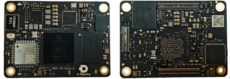
The RDK X5 Module serves as the core board, integrating the D-Robotics Sunrise®5 intelligent computing chip and its key circuitry, incorporating core functional units such as PMIC power management module, DDR, eMMC, QSPI NAND, Wi-Fi/Bluetooth, etc. The core board provides a 300-pin high-speed expansion interface, enabling flexible connection to various peripherals and meeting the rapid deployment needs across diverse application scenarios.
RDK X5 Module Carrier Board is a supporting IO carrier board for RDK X5 Module, providing a rich peripheral interface. Direct interfaces include:
Two 22-pin camera interfaces (integrated MIPI CSI, LPWM&MCLK, I²C, GPIO)
One HDMI interface
One RJ45 Ethernet interface
One LCD interface (integrated MIPI DSI and I²C)
40-pin expansion interface (including GPIO, I²C, SPI, I²S, PWM)
Multiple functional control interfaces, etc.
Interfaces processed by peripheral components on the IO carrier board and then output include:
CAN bus interface (using TCAN4550 chip, SPI-to-CAN)
Headphone audio interface (based on ES8326B, supporting I²S to audio DAC&ADC)
Four USB 3.0 interfaces (expanded via GL3510 USB Hub)
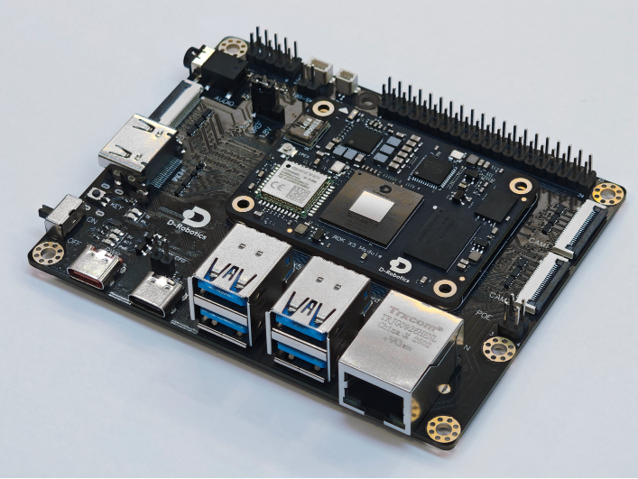
Users can refer to the circuit design of the IO carrier board to independently develop customized baseboards that meet their own application requirements.
2.3.1.2. Specifications
Basic specifications of X5 MD are as follows:
| Module | Parameter |
|---|---|
| Processor | Sunrise 5 (X5) Chip |
| CPU | 8-core ARM® Cortex® A55 @ 1.5GHz |
| BPU | Bayers-architecture BPU @ 1.0GHz, 10 TOPS |
| Storage | 2GB/4GB/8GB LPDDR4, 0/8GB/16GB/32GB/64GB eMMC |
| Camera | 2 x 4-lane MIPI CSI interfaces |
| Display | 1 x HDMI 1080P@60fps, 1 x MIPI DSI 2K@30fps |
| USB | 1 x USB Type-A 3.0 interface, 1 x Micro USB 2.0 interface |
| Wired Network | 1 x Gigabit Ethernet interface |
| Wireless Network | 2.4G / 5G Wi-Fi x1, supports 802.11 b/g/n, Bluetooth 5.1 |
| Other Interfaces | TF card interface x1, 40 PIN interface x1, I2S x2 |
| Power Supply | USB Type C 5V/5A power supply |
2.3.1.3. X5 MD Accessory Description
Before using the X5 MD development board, users need to prepare the following accessories:
Essential Accessories
USB Type-C 5V/5A power adapter
1 x Gigabit Ethernet cable, for network communication
1 x Micro USB 2.0 data cable, for serial communication
1 x USB Type-C data cable, for USB 2.0 data transfer
Camera module, for video and image function evaluation
Optional Accessories
Monitor and HDMI Type-A cable, for video preview
MIPI LCD display and 22-pin FPC, for display function testing
Audio sub-board, for voice function testing
2.3.2. IO Carrier Board Functional Module Layout
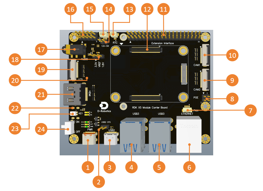
| Interface | Function | Interface | Function |
|---|---|---|---|
| 1 | USB Type C 5V/5A power supply interface | 13 | RTC battery interface |
| 2 | USB2.0 configuration header | 14 | CAN termination resistor switch |
| 3 | USB2.0 interface | 15 | CAN bus interface |
| 4 | USB3.0 HOST interface x2 | 16 | Functional control IO header |
| 5 | USB3.0 HOST interface x2 | 17 | Audio interface |
| 6 | Gigabit Ethernet port | 18 | IO voltage level selection header |
| 7 | Fan interface | 19 | MIPI DSI interface |
| 8 | POE interface | 20 | Micro SD card interface (back side) |
| 9 | CAM2 interface, 4-lane | 21 | HDMI interface |
| 10 | CAM1 interface, 4-lane | 22 | Debug port, USB-to-serial (back side) |
| 11 | 40-pin header | 23 | Sleep button |
| 12 | Core module interface | 24 | Power switch |
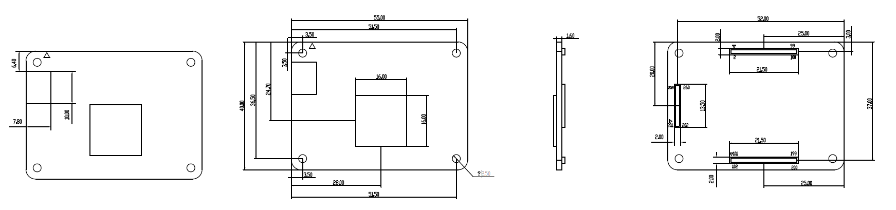
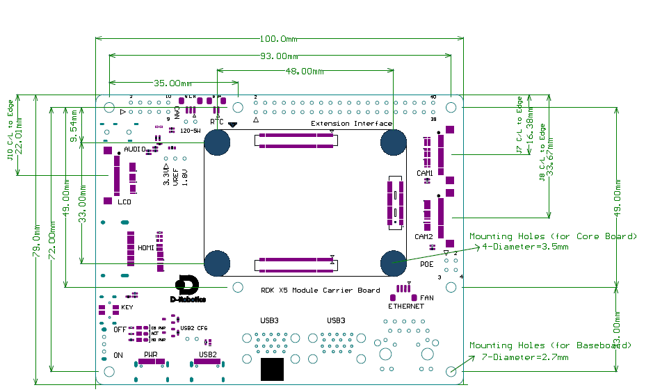
2.3.2.1. Dimension Diagram
2.3.3. Interface Usage Instructions
2.3.3.1. Powering On the Development Board
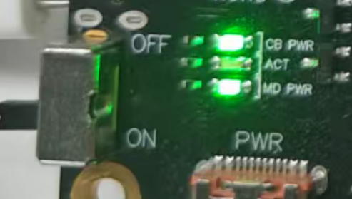
Connect the 5V/5A power adapter (interface 1), turn on the power switch (interface 24). When CB PWR and MD PWR lights up, it indicates the development board is powered normally.
2.3.3.2. Booting from eMMC
The X5 MD was initially designed for RDK ecosystem customers running the RDK system, booting from spi nand by default. If you need to flash and use the SDK system, you must change to boot from eMMC.
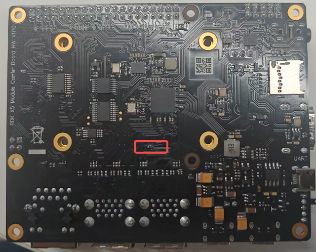
First, confirm the board’s hardware version using silkscreen markings on the core board and IO carrier board.
For version V0.X: you need to modify the core board; please contact FAE for the eMMC boot modification method;
For version V1.X: you need to modify the IO carrier board: solder a 4.7kΩ resistor at the position shown in the figure.
2.3.3.3. Debug Serial Port
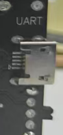
The development board provides one debug serial port (back side interface 22) for serial login and debugging. Configuration parameters for the computer’s serial tool are as follows:
Baud rate: 921600
Data bits: 8
Parity: None
Stop bits: 1
Flow control: None
To connect via serial, use a Micro-USB cable to connect development board interface 22 to the PC.
2.3.3.4. Ethernet
The development board provides 1 x RJ45 network interface, corresponding to interface 6, supporting 1000BASE-T, 100BASE-T, and 10BASE-T standards. The board’s default ip address is 192.168.1.10. To check the IP address, log in via serial and execute the ifconfig command to view information for the eth0 node.
root@buildroot:~$ ifconfig
eth0: flags=4163<UP,BROADCAST,RUNNING,MULTICAST>  mtu 1500
        inet 192.168.1.10  netmask 255.255.255.0  broadcast 0.0.0.0
        ether 9a:77:34:d1:fc:ed  txqueuelen 1000  (Ethernet)
        RX packets 1813  bytes 134485 (131.3 KiB)
        RX errors 0  dropped 1  overruns 0  frame 0
        TX packets 4563  bytes 282810 (276.1 KiB)
        TX errors 0  dropped 0 overruns 0  carrier 0  collisions 0
        device interrupt 38
Additionally, this interface supports PoE (Power over Ethernet), enabling simultaneous data and power transmission over a single Ethernet cable, simplifying and increasing flexibility in device installation.
2.3.3.5. USB 3.0 Interface
The development board provides 1 x USB 3.0 interface; the IO carrier board expands it into 4 x USB 3.0 Type-A interfaces (corresponding to interfaces 4 and 5), operating in Host mode by default.
If the user’s custom baseboard does not include a USB hub, the mode can be switched to Device mode via software.
Enable USB 3.0 Device Mode
Execute system configuration commands to forcibly switch the USB 3.0 master/slave mode.
Command to set USB 3.0 to Device mode:
echo device > /sys/class/usb_role/35100000.usb-role-switch/role
Command to set USB 3.0 to Host mode:
echo host > /sys/class/usb_role/35100000.usb-role-switch/role
2.3.3.6. USB 2.0 Interface
The development board provides 1 x Micro USB 2.0 interface (interface 3). Shorting interface 2 allows switching USB 2.0 to HOST mode.
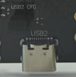
Main application functions of this interface include:
Functional debugging, default ADB mode, can switch to rndis, uvc, etc. via commands
Image flashing, supports flashing in dfu, fastboot, etc. modes
Peripheral access, flexible switching between host and device modes with interface 3
2.3.3.7. IO Voltage Level Selection
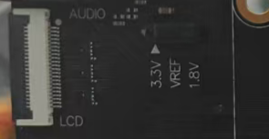
The development board provides one IO voltage level selection interface (interface 18), allowing switching between 1.8V or 3.3V. This setting affects the IO voltage levels of both the 40-pin interface and the CAM interface simultaneously.
2.3.3.8. Camera (MIPI CSI) Interface
The development board provides 2 x 22-pin MIPI CSI interfaces: CAM1 (interface 10), CAM2 (interface 9).
Capabilities and configurations of the two interfaces are listed below:
| Interface | MIPI CSI Host | Max Supported Lanes | I2C Bus | Reset GPIO | LPWM & MCLK |
|---|---|---|---|---|---|
| 10 | MIPI_CSI0&1 | 4 lane | I2C6 | LSIO_GPIO1_06 - 353 | LSIO_LPWM1_0 & LSIO_SENSOR0_MCLK |
| 9 | MIPI_CSI2&3 | 4 lane | I2C4 | LSIO_GPIO1_04 - 351 | LSIO_LPWM1_1 & LSIO_SENSOR1_MCLK |
The 22-pin interface can connect Raspberry Pi-style camera modules. The IO voltage (interface 18) should be set to 3.3V. Supported modules include IMX219, IMX477, OV5647, with MCLK provided by the module.
An official 22-pin to 24-pin adapter board is provided, which integrates a 24MHz active crystal to provide MCLK for the sensor. The IO voltage (interface 18) should be set to 1.8V.
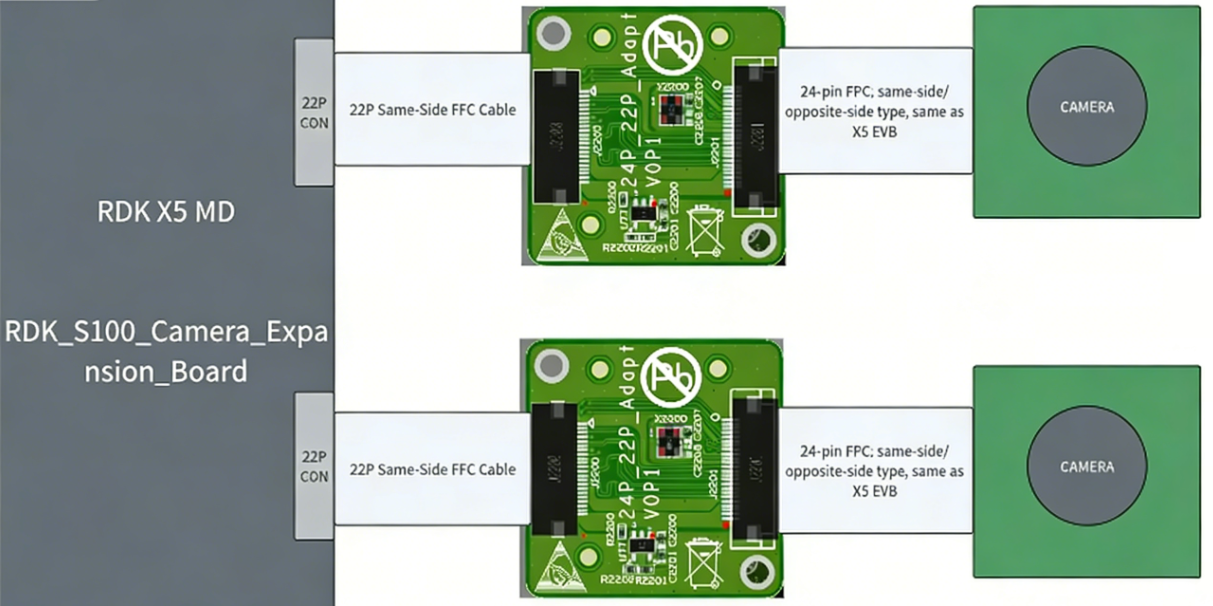
The X5 MD connects to the adapter board via a 22-pin 0.5mm pitch same-direction FPC, and the adapter board connects to the camera module using the same type of ribbon cable as the EVB board.
Using the adapter board, a series of camera modules supported by the EVB board can be connected, such as SC230AI, SC132gs, IMX415, facilitating user testing under various imaging scenarios. For a complete list of supported Camera Sensors, please refer to Camera Sensor Support List.
After installation, use commands to confirm whether the module’s I2C address can be detected normally. If not detected, check the FPC connection for issues such as poor contact or reversed orientation.
Query I2C device address of Camera Sensor on CAM1 (interface 10):
echo 353 > /sys/class/gpio/export
echo out > /sys/class/gpio/gpio353/direction
echo 0 > /sys/class/gpio/gpio353/value
sleep 0.1
echo 1 > /sys/class/gpio/gpio353/value

i2cdetect -y -r 6
Query I2C device address of Camera Sensor on CAM2 (interface 9):
echo 351 > /sys/class/gpio/export
echo out > /sys/class/gpio/gpio351/direction
echo 0 > /sys/class/gpio/gpio351/value
sleep 0.1
echo 1 > /sys/class/gpio/gpio351/value

i2cdetect -y -r 4
When the Camera Sensor’s I2C device address is successfully detected, output will appear as shown below (example detecting SC230AI on interface 10, where address 30 is printed):
root@buildroot:~$ i2cdetect -y -r 6
     0  1  2  3  4  5  6  7  8  9  a  b  c  d  e  f
00:                         -- -- -- -- -- -- -- --
10: -- -- -- -- -- -- -- -- -- -- -- -- -- -- -- --
20: -- -- -- -- -- -- -- -- -- -- -- -- -- -- -- --
30: 30 -- -- -- -- -- -- -- -- -- -- -- -- -- -- --
40: -- -- -- -- -- -- -- -- -- -- -- -- -- -- -- --
50: -- -- -- -- -- -- -- -- -- -- -- -- -- -- -- --
60: -- -- -- -- -- -- -- -- -- -- -- -- -- -- -- --
70: -- -- -- -- -- -- -- --
For more information on Camera Sensor usage, please refer to Example Code Introduction.
2.3.3.9. HDMI Interface
The development board supports 1 x HDMI Type-A interface (interface 21), with supported Pixel Clock range from 25 MHz to 165 MHz.
Since the system does not support a graphical interface, the HDMI interface is primarily used for real-time preview of camera and network stream images. For specific methods, please refer to display-related examples in Example Code Introduction.
2.3.3.10. LCD (MIPI DSI) and TP Interface
The development board supports MIPI DSI and touchscreen interfaces (interface 19), a 22-pin connector. It can use DSI-Cable-12cm to connect to a Waveshare 4.3-inch capacitive touchscreen with 800×480 resolution, as shown below:
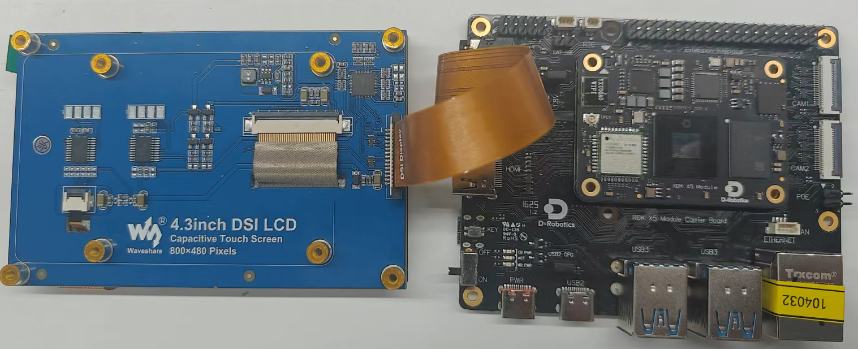
After successfully entering the Linux system, execute the following commands to load drivers:
modprobe sii902x
modprobe panel-wh-cm480
modprobe ft5406
modprobe hb_bl
modprobe vio_n2d
modprobe vs-x5-syscon-bridge
modprobe vs_drm
The serial console will print:
[ 3343.383052] vs-disp-sif 3e080000.vs-sif: Adding to iommu group 3
[ 3343.384118] vs-dc 3e000000.dc8000Nano: Adding to iommu group 4
[ 3343.385252] vs-bt1120 3e010000.bt1120: Adding to iommu group 5
[ 3343.387555] horizon-lsio-pinctrl 34180000.lsio_iomuxc: set pin = 14 direction to input
[ 3343.387567] horizon-lsio-pinctrl 34180000.lsio_iomuxc: map pin14 to gpio[0] - 14
[ 3343.387635] panel-jc-050hd134 3e060000.mipi_dsi0.0: supply power not found, using dummy regulator
[ 3343.391241] vs-drm 3e000000.disp_apb:display-subsystem: bound 3e080000.vs-sif (ops sif_component_ops [vs_drm])
[ 3343.391529] vs-drm 3e000000.disp_apb:display-subsystem: bound 3e000000.dc8000Nano (ops dc_component_ops [vs_drm])
[ 3343.391692] vs-drm 3e000000.disp_apb:display-subsystem: bound 3e010000.bt1120 (ops bt1120_component_ops [vs_drm])
[ 3343.391730] vs-drm 3e000000.disp_apb:display-subsystem: bound 3e000000.disp_apb:bt1120_bridge (ops bt1120_bridge_component_ops [vs_drm])
[ 3343.391764] vs-drm 3e000000.disp_apb:display-subsystem: bound 3e000000.disp_apb:bt1120_bridge_wb (ops bt1120_bridge_component_ops [vs_drm])
[ 3343.391816] vs-drm 3e000000.disp_apb:display-subsystem: bound 3e060000.mipi_dsi0 (ops dsi_component_ops [vs_drm])
[ 3343.391917] vs-drm 3e000000.disp_apb:display-subsystem: bound 3e000000.disp_apb:dsi-encoder (ops encoder_component_ops [vs_drm])
[ 3343.391976] vs-drm 3e000000.disp_apb:display-subsystem: bound 3e000000.disp_apb:hdmi-encoder (ops encoder_component_ops [vs_drm])
[ 3343.392815] [drm] Initialized vs-drm 1.0.0 20191101 for 3e000000.disp_apb:display-subsystem on minor 0
play-subsystem on minor 0
Appearance of [drm] Initialized vs-drm 1.0.0 20191101 for 3e000000.disp_apb:display-subsystem on minor 0 indicates successful display driver loading.
Use the command modetest -M vs-drm -a -s 73@31:800x480 -P 33@31:800x480@NV12 for testing.
The connected screen will light up, displaying a pattern as shown below:
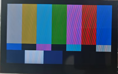
In the driver loading command, ft5406 is the touchscreen driver, and hb_bl is the backlight driver. For specific driver development, please refer to the touchscreen user manual and Driver Development Guide.
After successful driver loading, the /dev/input/event1 device node will be created for user-space applications.
Testing Usage:
Use the tc_test program to test touchscreen functionality. When touching the screen, events, types, status codes, and corresponding coordinates can be obtained.
# ./tc_test /dev/input/event1
Monitoring input events on /dev/input/event1
[/dev/input/event1] event(0): type:3; code: 47; value:  0; realx:  0; realy:  0
[/dev/input/event1] event(1): type:3; code: 57; value: 16; realx:  0; realy:  0
[/dev/input/event1] event(2): type:3; code: 53; value:248; realx:248; realy:  0
[/dev/input/event1] event(3): type:3; code: 54; value:1007; realx:248; realy:1007
[/dev/input/event1] event(4): type:3; code: 48; value: 13; realx:248; realy:1007
[/dev/input/event1] event(5): type:3; code: 58; value: 13; realx:248; realy:1007
Test Code:
#include <stdio.h>
#include <stdlib.h>
#include <fcntl.h>
#include <unistd.h>
#include <linux/input.h>

static int handle_event(int fd, const char *device_name)
{
	struct input_event ev[64];
	int button = 0, realx = 0, realy = 0, i, rd;

	rd = read(fd, ev, sizeof(struct input_event) * 64);
	if (rd < (int)sizeof(struct input_event)) return 0;

	for (i = 0; i < rd / (int)sizeof(struct input_event); i++)
	{
		if (EV_ABS == ev[i].type)
		{
			if (ev[i].code == 53) {
				realx = ev[i].value;
			} else if (ev[i].code == 54) {
				realy = ev[i].value;
			}
		}
		printf("[%s] event(%d): type:%d; code:%3d; value:%3d; realx:%3d; realy:%3d\n",
			   device_name, i, ev[i].type, ev[i].code, ev[i].value, realx, realy);
	}
	return 1;
}

int main(int argc, char *argv[])
{
	if (argc < 2) {
		printf("Usage: %s <event device path>\n", argv[0]);
		return -1;
	}

	const char *device_path = argv[1];
	int fd = open(device_path, O_RDONLY);
	if (fd < 0) {
		printf("Failed to open input device: %s\n", device_path);
		return -1;
	}

	printf("Monitoring input events on %s\n", device_path);
	while (handle_event(fd, device_path));

	close(fd);
	return 0;
}
2.3.3.11. Wi-Fi antenna
Development boards of V1P1 and previous versions support two configuration methods: onboard antenna and external antenna in wireless network design. The default is the onboard antenna, and the antenna channel can be switched through GPIO control.
#Antenna control initialization
echo 428 > /sys/class/gpio/export
echo 429 > /sys/class/gpio/export
echo out > /sys/class/gpio/gpio428/direction
echo out > /sys/class/gpio/gpio429/direction

#Switch to onboard antenna
echo 1 > /sys/class/gpio/gpio428/value
echo 0 > /sys/class/gpio/gpio429/value

#Switch to external antenna
echo 0 > /sys/class/gpio/gpio428/value
echo 1 > /sys/class/gpio/gpio429/value
2.3.3.12. Wi-Fi / Bluetooth
Using Wi-Fi
The development board integrates an FCS960K 2.4G/5.0G dual-mode Wi-Fi/Bluetooth module, supporting IEEE802.11a/b/g/n/ac/ax WLAN and Bluetooth 5.1 functions. The Wi-Fi driver is automatically loaded upon system startup.
root@buildroot:~$ ifconfig wlan0
wlan0: flags=4098<BROADCAST,MULTICAST>  mtu 1500
        ether 40:9c:a7:70:98:cc  txqueuelen 1000  (Ethernet)
        RX packets 0  bytes 0 (0.0 B)
        RX errors 0  dropped 0  overruns 0  frame 0
        TX packets 0  bytes 0 (0.0 B)
        TX errors 0  dropped 0 overruns 0  carrier 0  collisions 0
Users need to manually configure the SSID and IP address by modifying configuration files as follows:
# Enter userdata directory to avoid file write errors in system directories
cd /userdata/
# Modify the SSID ("WIFI_SSID") and password ("WIFI_PASSWD") in the command according to your Wi-Fi network
wpa_passphrase "WIFI_SSID" "WIFI_PASSWD"  >> ./wpa_supplicant.conf

sleep 1
wpa_supplicant -D nl80211 -i wlan0 -c ./wpa_supplicant.conf -B
sleep 1
udhcpc -i wlan0 &
After configuration, execute ping 8.8.8.8 to confirm network connectivity. Normal log output is as follows:
root@buildroot:~$ cd /userdata/
root@buildroot:/userdata$ wpa_passphrase WiFi-Test 12345678 >> ./wpa_supplicant.conf
root@buildroot:/userdata$ wpa_supplicant -D nl80211 -i wlan0 -c ./wpa_supplicant.conf -B
Successfully initialized wpa_supplicant
[10093.447698] [BB][halbb_la_bb_set_smp_rate] smp_rate_tmp=7, la_smp_rate_log=160 M
root@buildroot:/userdata$ udhcpc -i wlan0 &
[1] 1309
udhcpc: started, v1.35.0
root@buildroot:/userdata$ udhcpc: broadcasting discover
udhcpc: broadcasting select for 192.168.137.252, server 192.168.137.1
udhcpc: lease of 192.168.137.252 obtained from 192.168.137.1, lease time 604800
deleting routers
adding dns 192.168.137.1

[1]+  Done                    udhcpc -i wlan0
root@buildroot:/userdata$ ifconfig wlan0
wlan0: flags=4163<UP,BROADCAST,RUNNING,MULTICAST>  mtu 1500
        inet 192.168.137.252  netmask 255.255.255.0  broadcast 192.168.137.255
        ether 40:9c:a7:70:98:cc  txqueuelen 1000  (Ethernet)
        RX packets 117  bytes 15326 (14.9 KiB)
        RX errors 0  dropped 1  overruns 0  frame 0
        TX packets 63  bytes 5056 (4.9 KiB)
        TX errors 0  dropped 0 overruns 0  carrier 0  collisions 0

root@buildroot:/userdata$ ping 8.8.8.8
PING 8.8.8.8 (8.8.8.8): 56 data bytes
64 bytes from 8.8.8.8: seq=0 ttl=52 time=82.124 ms
64 bytes from 8.8.8.8: seq=1 ttl=52 time=106.029 ms
64 bytes from 8.8.8.8: seq=2 ttl=52 time=129.993 ms
^ C
--- 8.8.8.8 ping statistics ---
3 packets transmitted, 3 packets received, 0% packet loss
round-trip min/avg/max = 82.124/106.048/129.993 ms
root@buildroot:/userdata$
Switching between Wi-Fi STA and AP modes:
Execute /etc/init.d/wifi_init.sh ap to switch to AP mode, and /etc/init.d/wifi_init.sh sta to switch to STA mode.
root@buildroot:~# /etc/init.d/wifi_init.sh ap
Initialize wlan0 to ap mode
wlan0: interface state UNINITIALIZED->ENABLED
wlan0: AP-ENABLED
Finish initialize wlan0 to ap mode
dnsmasq: started, version 2.86 cachesize 150
root@buildroot:~# dnsmasq: compile time options: IPv6 GNU-getopt DBus no-UBus no-i18n no-IDN DHCP DHCPv6 no-Lua TFTP no-conntrack ipset auth no-cryptohash no-DNSSEC loop-detect inotify dumpfile
dnsmasq: warning: no upstream servers configured
dnsmasq-dhcp: DHCP, IP range 192.168.5.2 -- 192.168.5.254, lease time 12h
dnsmasq: read /etc/hosts - 2 addresses

root@buildroot:~# /etc/init.d/wifi_init.sh sta
Initialize wlan0 to station mode
Finish initialize wlan0 to station mode
Using Bluetooth
Execute /etc/init.d/bt_init.sh to complete Bluetooth initialization.
Execute bluetoothctl to enter the interactive Bluetooth configuration interface. If device information similar to the image below appears, the Bluetooth has been recognized. Then use show to view Bluetooth information, paying attention to the powered and discoverable states.
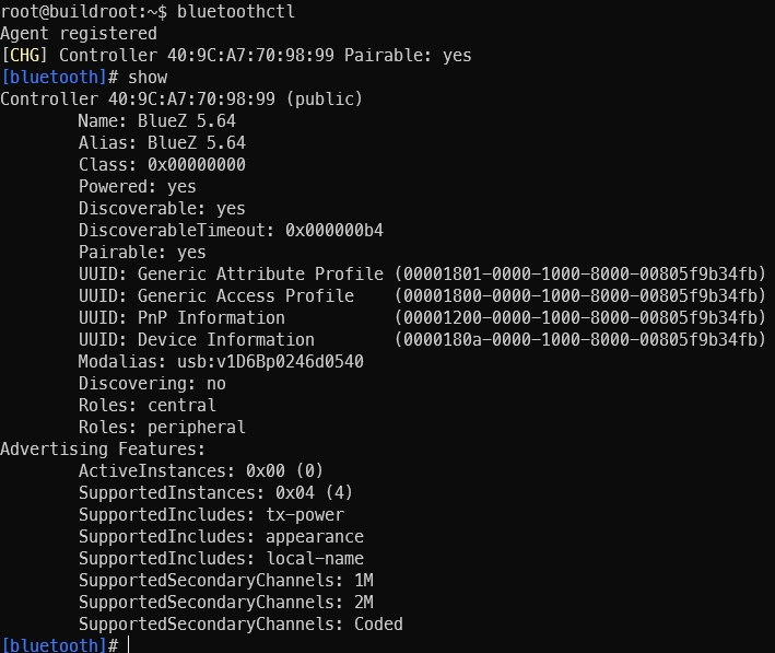
Execute power on to enable Bluetooth, as shown below:

To make the Bluetooth discoverable by nearby devices, execute discoverable on to enable the discoverable property, as shown below:

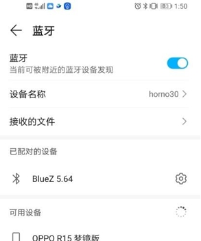
Now, using a phone or computer to scan Bluetooth will reveal a device named BlueZ 5.64 (the version number in the name may vary depending on the BlueZ version, e.g., BlueZ 5.79):
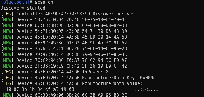
Next, test Bluetooth’s active scanning function: in the bluetoothctl interactive interface, input scan on to start active scanning. It will periodically print nearby devices. You can see my phone has been discovered. Use scan off to stop scanning and summarize the discovered Bluetooth devices:
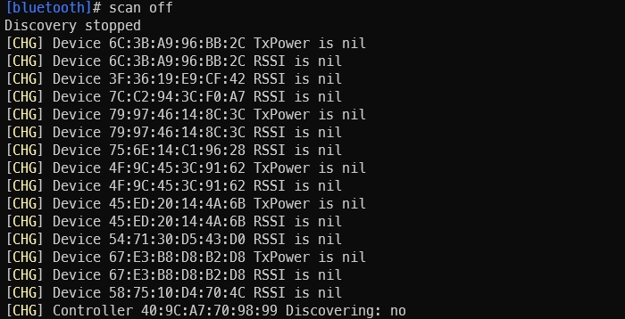
Then proceed to pair with other Bluetooth devices:
Pairing command: pair [targetMAC]. After entering this command, type yes when prompted, and select “Pair” on the target Bluetooth device to complete pairing.
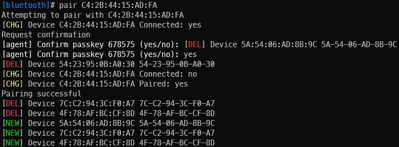
After successful pairing, use trust [targetMAC] to enable automatic connection next time.
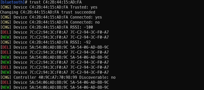
Use l2ping to test network connectivity.
2.3.3.13. TF Card
The development board supports one TF card interface (Interface 22), with maximum support for SDR104 mode. It supports file system formats including FAT32 (VFAT), EXFAT, ext2, ext3, and ext4.
After inserting the TF card, the kernel outputs logs similar to the following, indicating successful recognition:
[ 9809.931894] mmc1: new HSSDHC card at address 1234
[ 9809.933740] mmcblk1: mmc1:1234 SA16G 14.5 GiB
[ 9809.940060]  mmcblk1: p1
Note: Actual log output may vary slightly depending on the specific model and partitioning of the TF card.
If the file system format of the TF card partition is not FAT32 (VFAT), ext2, ext3, or ext4, use the following commands to format the TF card partition:
# Format as FAT32 (VFAT)
mkfs.vfat /dev/mmcblk2p1
# Format as ext4
mkfs.ext4 /dev/mmcblk2p1
# Format as ext3
mkfs.ext3 /dev/mmcblk2p1
# Format as ext2
mkfs.ext2 /dev/mmcblk2p1
2.3.3.14. CANFD Interface
The development board provides a CANFD interface (Interface 15) and a CAN termination resistor switch (Interface 14). For high-speed communication, termination resistors should be enabled at both ends to prevent signal reflection and improve noise immunity. This interface supports both CAN and CAN FD communication.
The three signal pins of the CANFD interface are GND, L, and H.

2.3.3.15. 40PIN Interface
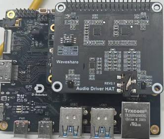
The development board provides one 40PIN interface (Interface 11), allowing users to expand peripheral connections. The pin definitions and supported multiplexing functions are shown below:
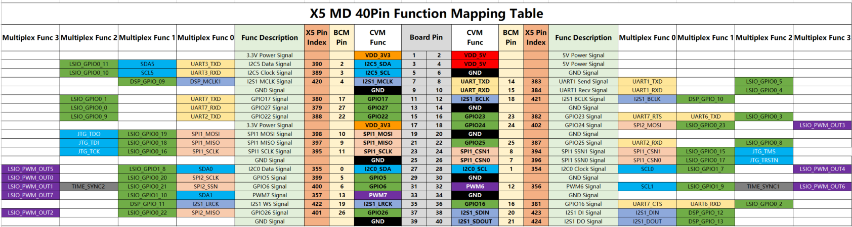
All IO pins on the 40PIN interface support voltage domain selection (3.3V or 1.8V) via the voltage selection interface (Interface 18).
Connection Example:
Below is a hardware reference connection diagram for an Audio Driver HAT:
2.3.3.16. RTC
The development board enables the RTC function of the PMIC chip hpu3501. The RTC battery interface is Interface 13:

From left to right, the connector pins are: battery negative, battery positive. Requirements for battery voltage and discharge current are: 2–3.3V, >2.5uA.
The hpu3501-rtc is registered as rtc0. You can use the following commands to test the external RTC:
# Confirm the existence of /dev/rtc0 device
ls /dev/rtc*

# Create a soft link from /dev/rtc0 to /dev/rtc
rm /dev/rtc
ln -s /dev/rtc0 /dev/rtc

# Write time to external RTC
date -s "2024/01/01 17:08:00"    # Set system time
hwclock -w                       # Write system time to RTC
hwclock -r                       # Read RTC time to verify successful write

# After rebooting, read time from external RTC to system
# Confirm the existence of /dev/rtc0 device
ls /dev/rtc*
# Create a soft link from /dev/rtc0 to /dev/rtc
rm /dev/rtc
ln -s /dev/rtc1 /dev/rtc
hwclock -s                               # If the RTC battery is present, after power-off and re-powering, the RTC time will be updated to system time
date                                     # Read system time; it should now be the previously set time "2024/01/01 17:08:00"
2.3.3.17. Other Interfaces
Power Switch
Controls power-on and power-off of the board. Corresponds to Interface 24.
Reset Switch
Performs full board power-down. The leftmost button of Interface 22 is for full board reset; the second button from the left is for X5MD module power-down.
Wake-up Switch
Used to wake up the system from Sleep mode via an external wake-up source. Corresponds to Interface 23.