2.1. X5 EVB 1_B Development Board User Guide
2.1.1. Functional Overview
2.1.1.1. Specifications
The X5 EVB development board serves as a reference platform for the X5 chip, providing various peripheral interfaces such as Ethernet, USB, Camera, LCD, HDMI, and 40PIN. Combined with peripheral accessories like cameras, audio boards, and LCD screens, users can conveniently evaluate and develop image, multimedia, and algorithm applications.
Basic specifications of the development board are as follows:
| Module | Parameters |
|---|---|
| Processor | Sunrise 5 (X5) chip |
| CPU | 8-core ARM® Cortex® A55@1.5GHz |
| BPU | Bayers-architecture BPU@1.0GHz, 10 TOPS |
| Memory | 2GB/4GB LPDDR4, 8GB/16GB eMMC |
| Camera | 1 x 4-lane MIPI CSI interface (can be split into 2 x 2-lane MIPI CSI via expansion board) 2 x 2-lane MIPI CSI interfaces |
| Display | 1 x HDMI 4K@30fps, 1 x MIPI DSI 2K@30fps |
| USB | 1 x USB Type-A 3.0 interface, 1 x Micro USB 2.0 interface |
| Wired Network | 1 x Gigabit Ethernet interface |
| Wireless Network | 2.4G / 5G Wi-Fi x1, supports 802.11 b/g/n, Bluetooth 5.1 |
| Other Interfaces | TF card interface x1, 40PIN interface x1, ADC x5, I2S0&PDM x1 |
| Power Supply | DC 12V adapter power input |
2.1.1.2. X5 EVB Accessories Description
Before using the X5 EVB development board, the following accessories are required:
Mandatory Accessories
12V power adapter x1, with at least 2A output capability
Gigabit Ethernet cable x1, for network communication
Micro USB 2.0 data cable x2, used separately for serial port and USB communication
Camera module, for video and image function evaluation
Optional Accessories
Monitor with HDMI Type-A cable, for video preview
MIPI LCD display and 24PIN FPC, for display function testing
Audio sub-board, for voice function testing
2.1.2. Function Module Layout
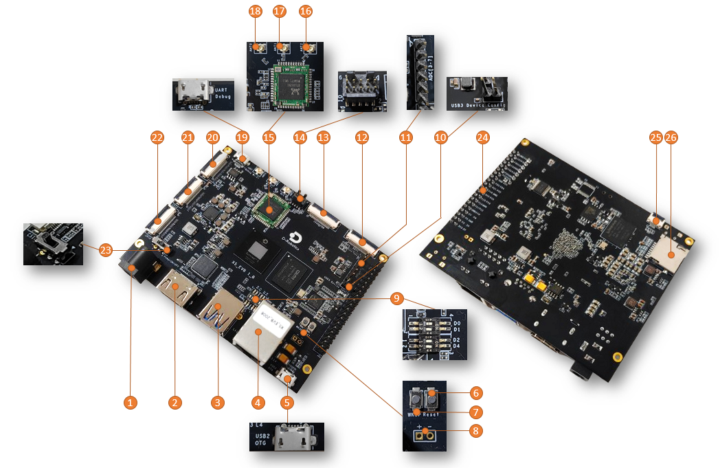
| Interface | Function | Interface | Function |
|---|---|---|---|
| 1 | 12V DC power adapter input | 14 | JTAG debug interface |
| 2 | HDMI Type-A interface, supports up to 4K@30 output | 15 | Wi-Fi and Bluetooth module, CDW-47852BS |
| 3 | USB 3.0 Type-A interface | 16 | Bluetooth antenna interface |
| 4 | Gigabit Ethernet interface | 17 | Wi-Fi antenna interface, Duplex supports simultaneous transmission of 2.4G&5G signals |
| 5 | Micro USB 2.0 data interface | 18 | Wi-Fi antenna interface, Duplex supports simultaneous transmission of 2.4G&5G signals |
| 6 | Reset button | 19 | Micro USB 2.0 debug serial port |
| 7 | Wake-up button | 20 | 4-lane MIPI CSI interface (can be split into 2 x 2-lane MIPI CSI via expansion board) |
| 8 | RTC external power supply interface | 21 | 2-lane MIPI CSI interface |
| 9 | Boot configuration DIP switch, for selecting boot mode | 22 | 2-lane MIPI CSI interface |
| 10 | USB 3.0 host/device mode switching interface | 23 | Power switch |
| 11 | ADC[3-7] functional pins | 24 | 40PIN functional pins, support UART, I2C, SPI, PWM, I2S |
| 12 | 4-lane MIPI DSI interface | 25 | Independent I2C interface, can be extended to MIPI CSI interface |
| 13 | I2S&PDM audio interface | 26 | TF card interface |
2.1.2.1. Dimension Diagram
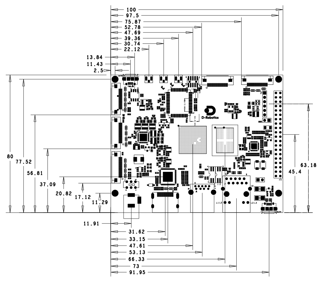
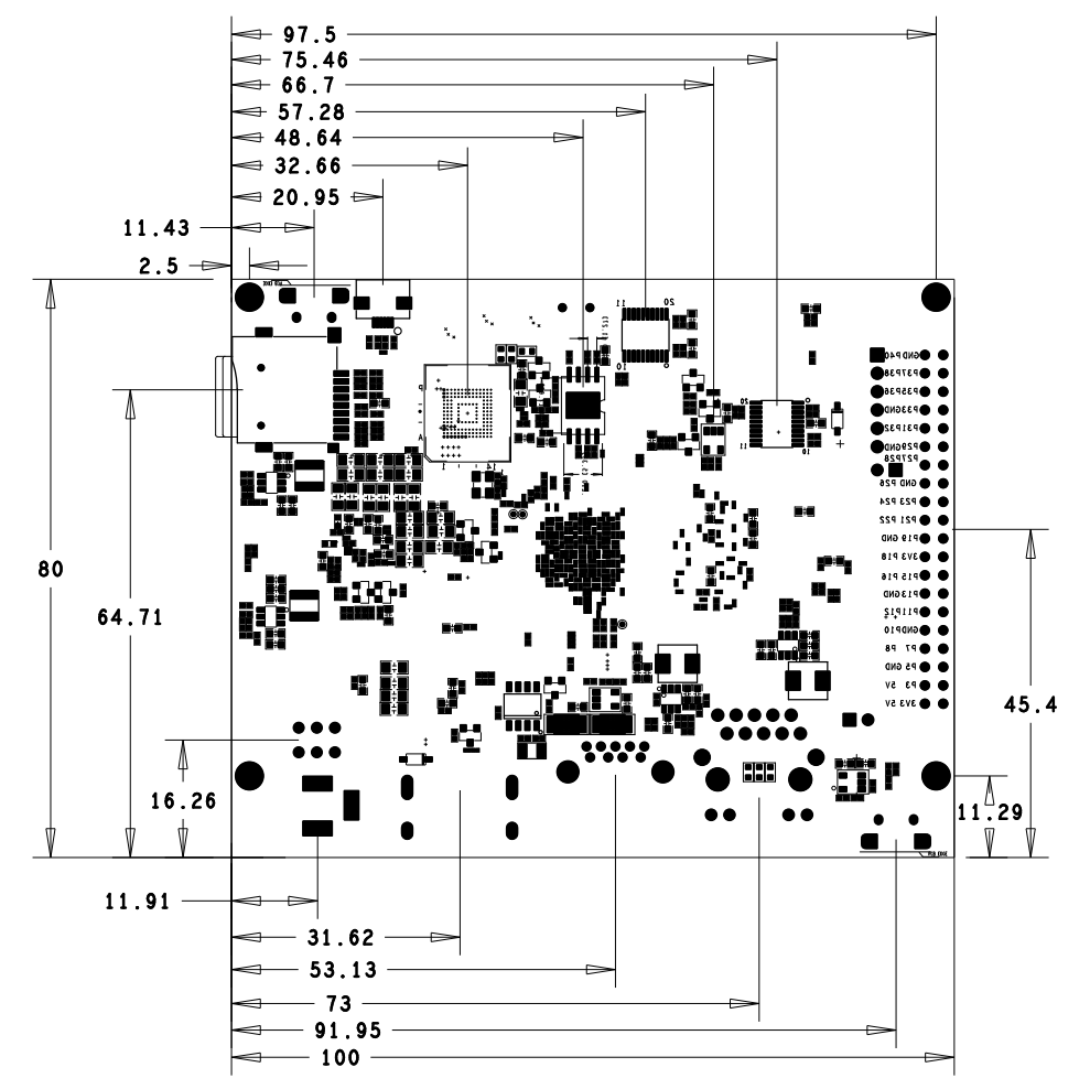
2.1.3. Interface Usage Instructions
2.1.3.1. Starting the Development Board
Please follow the steps below to set up and power on the development board.
Before powering on, ensure the boot configuration DIP switch (interface 9) is set to D0: ON, D1/D2/D4: OFF, indicating boot from
eMMCwith serial port baud rate115200, as shown in the figure below: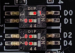
Connect the 12V power adapter (interface 1), turn on the power switch (interface 23). The red indicator light should illuminate, indicating normal power supply.
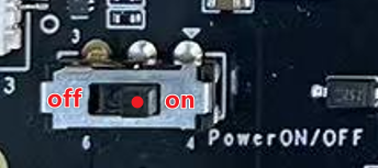
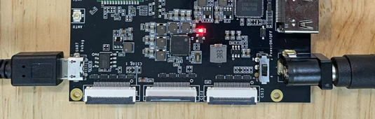
Note: If the power LED is lit but no output appears on the debug serial port, verify the DIP switch settings.
2.1.3.2. DIP Switch
The DIP switch (interface 9) determines the boot mode and debug serial port baud rate, allowing users to configure the development board for different operating modes.
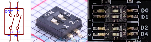
The internal structure and physical appearance of the DIP switch are shown below. Setting a switch to ON indicates a high-level signal 1.
DIPs
D0, D1, D2correspond to the2NDBOOT_SELpins of the X5 chip, used to determine the boot mode.DIP
D4corresponds to theUART_BPSpin of the X5 chip, used to set the debug serial port baud rate.
The corresponding truth table for the DIP switch is as follows:
| 2NDBOOT_SEL | Value | Option | Boot Mode Description |
|---|---|---|---|
| D2, D1, D0 | 000 | 2NDBOOT UART | Boot via UART interface |
| 001 | 2NDBOOT eMMC | Boot from eMMC storage device | |
| 010 | 2NDBOOT USB2.0 DFU | Boot via USB2.0 DFU (Device Firmware Upgrade) interface, via Dp/Dm | |
| 011 | 2NDBOOT SD Card | Boot from SD card | |
| 100 | 2NDBOOT QSPI NOR Flash | Boot from QSPI NOR Flash storage device | |
| 101 | 2NDBOOT QSPI NAND Flash | Boot from QSPI NAND Flash storage device | |
| 110 | 2NDBOOT USB3.0 DFU | Boot via USB3.0 DFU (Device Firmware Upgrade) interface, via Dp/Dm | |
| 111 | 2NDBOOT QSPI NAND Flash (disable mmu) | Boot from QSPI NAND Flash storage device with MMU disabled |
Note: X5 burning only supports the USB 2.0 protocol. Regardless of whether the USB 2.0 or USB 3.0 interface is used, it is burned according to the USB 2.0 protocol, and the maximum speed is 480Mbps.
| UART_BPS | Value | Option | Description |
|---|---|---|---|
| D4 | 0 | 115200bps | Debug serial port baud rate set to 115200bps |
| 1 | 921600bps | Debug serial port baud rate set to 921600bps |
2.1.3.3. Debug Serial Port
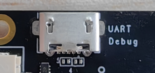
The development board provides 1 debug serial port, corresponding to interface 19. The board uses a CH340N USB-to-serial chip to convert the serial signal to a USB interface. Users can connect a Micro USB data cable to enable serial communication between the PC and the development board.
2.1.3.4. Ethernet
The development board provides 1 RJ45 network interface (interface 4), supporting 1000BASE-T, 100BASE-T, and 10BASE-T standards. The default ip address is 192.168.1.10. To check the IP address, log in via the serial port and execute the ifconfig command to view information for the eth0 node.
root@buildroot:~$ ifconfig
eth0: flags=4163<UP,BROADCAST,RUNNING,MULTICAST>  mtu 1500
        inet 192.168.1.10  netmask 255.255.255.0  broadcast 0.0.0.0
        ether 9a:77:34:d1:fc:ed  txqueuelen 1000  (Ethernet)
        RX packets 1813  bytes 134485 (131.3 KiB)
        RX errors 0  dropped 1  overruns 0  frame 0
        TX packets 4563  bytes 282810 (276.1 KiB)
        TX errors 0  dropped 0 overruns 0  carrier 0  collisions 0
        device interrupt 38
2.1.3.5. USB 3.0 Interface
The development board provides 1 USB 3.0 Type-A interface (interface 3), defaulting to Host mode. Users can switch to Device mode using the following methods.
Enable USB 3.0 Device Mode
USB 3.0 can be set to Device mode via software or hardware methods.
Hardware Method
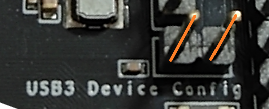
Short-circuit the pins of interface 10 to automatically switch USB 3.0 to Device mode. Disconnecting the short will return it to Host mode.
Software Method
Use system commands to force switching between Host and Device modes.
Command to set USB 3.0 to Device mode:
echo device > /sys/class/usb_role/35100000.usb-role-switch/role
Command to set USB 3.0 to Host mode:
echo host > /sys/class/usb_role/35100000.usb-role-switch/role
2.1.3.6. USB 2.0 Interface
The development board provides 1 Micro USB 2.0 interface (interface 5), supporting OTG functionality.
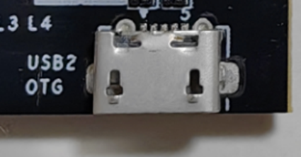
Main applications of this interface include:
Function debugging, defaulting to adb mode; can switch to rndis, uvc, etc., via commands
Image flashing, supporting dfu, fastboot, and other flashing modes
Peripheral connection, enabling various USB peripherals via OTG cable
2.1.3.7. Camera (MIPI CSI) Interface
The development board provides 3 MIPI CSI interfaces, corresponding to interfaces 20, 21, and 22.
Capabilities and configurations of the three interfaces are listed in the table below:
| Interface | MIPI CSI Host | Max Lanes Supported | I2C Bus | Reset GPIO |
|---|---|---|---|---|
| 20 | MIPI_CSI0&1 | 4 lanes | I2C4 | AON_GPIO_PIN0 - 498 |
| 21 | MIPI_CSI2 | 2 lanes | I2C2 | AON_GPIO_PIN4 - 502 |
| 22 | MIPI_CSI3 | 2 lanes | I2C7 | LSIO_GPIO1_06 - 353 |
Note: Interface 20’s MIPI CSI0&1 can be split into two 2-lane MIPI CSI interfaces (MIPI CSI0 and MIPI CSI1) using an external expansion board.
The board currently supports multiple camera modules including SC230AI, SC132gs, IMX415, etc., to meet various image testing requirements. For the complete list of supported Camera Sensors, refer to Camera Sensor Support List.
Camera modules connect to the board’s camera interface via a 24PIN FPC cable. Pay attention to the correct orientation when connecting, as shown in the figure below:
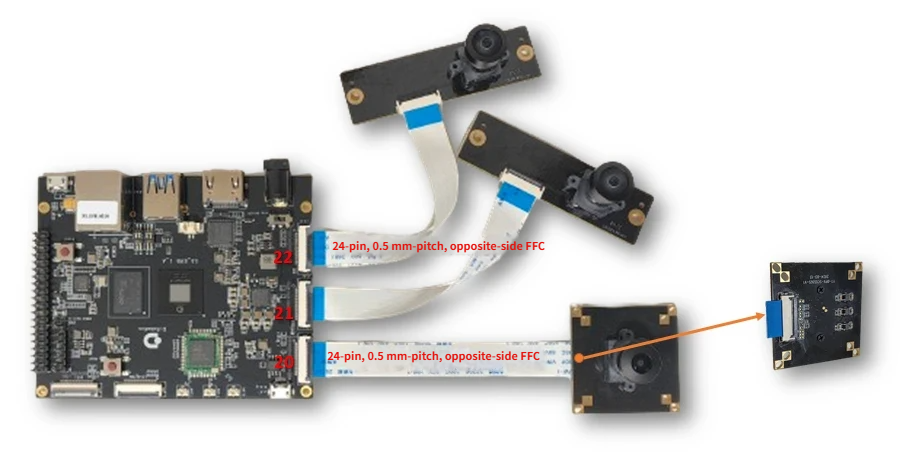
The number of MIPI lanes used by the camera module is the sole factor determining interface selection. Examples:
The
SC132gsmodule uses 2 lanes, so it can be connected to any of interfaces 20, 21, or 22.The
IMX415module uses 4 lanes, so it can only be connected to the 4-lane interface, i.e., interface 20.
After installation, use commands to verify if the module’s I2C address is detected. If not detected, check the FPC connection for issues such as poor contact or reversed orientation.
Query I2C address of Camera Sensor on interface 20:
echo 498 > /sys/class/gpio/export
echo out > /sys/class/gpio/gpio498/direction
echo 0 > /sys/class/gpio/gpio498/value
sleep 0.1
echo 1 > /sys/class/gpio/gpio498/value
echo 24000000 > /sys/class/vps/mipi_host0/param/snrclk_freq
echo 1 > /sys/class/vps/mipi_host0/param/snrclk_en

i2cdetect -y -r 4
Query I2C address of Camera Sensor on interface 21:
echo 502 > /sys/class/gpio/export
echo out > /sys/class/gpio/gpio502/direction
echo 0 > /sys/class/gpio/gpio502/value
sleep 0.1
echo 1 > /sys/class/gpio/gpio502/value
echo 24000000 > /sys/class/vps/mipi_host2/param/snrclk_freq
echo 1 > /sys/class/vps/mipi_host2/param/snrclk_en

i2cdetect -y -r 2
Query I2C address of Camera Sensor on interface 22:
echo 353 > /sys/class/gpio/export
echo out > /sys/class/gpio/gpio353/direction
echo 0 > /sys/class/gpio/gpio353/value
sleep 0.1
echo 1 > /sys/class/gpio/gpio353/value
echo 24000000 > /sys/class/vps/mipi_host3/param/snrclk_freq
echo 1 > /sys/class/vps/mipi_host3/param/snrclk_en

i2cdetect -y -r 7
Upon successful detection of the Camera Sensor’s I2C address, output similar to the following will appear (example: detecting SC230AI on interface 22, where address 30 is detected):
root@buildroot:~$ i2cdetect -y -r 7
     0  1  2  3  4  5  6  7  8  9  a  b  c  d  e  f
00:                         -- -- -- -- -- -- -- --
10: -- -- -- -- -- -- -- -- -- -- -- -- -- -- -- --
20: -- -- -- -- -- -- -- -- -- -- -- -- -- -- -- --
30: 30 -- -- -- -- -- -- -- -- -- -- -- -- -- -- --
40: -- -- -- -- -- -- -- -- -- -- -- -- -- -- -- --
50: -- -- -- -- -- -- -- -- -- -- -- -- -- -- -- --
60: -- -- -- -- -- -- -- -- -- -- -- -- -- -- -- --
70: -- -- -- -- -- -- -- --
For more information on Camera Sensor usage, please refer to Sample Code Introduction.
2.1.3.8. HDMI Interface
The development board supports 1 HDMI Type-A interface (interface 2), with maximum output resolution of 3840x2160@30fps.
Since the system does not support a graphical interface, the HDMI interface is primarily used for real-time preview of camera or network stream video. Specific methods are described in Sample Code Introduction under display-related examples.
2.1.3.9. LCD (MIPI DSI) and TP Interface
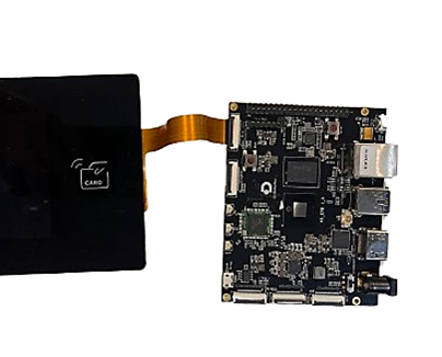
The development board supports MIPI DSI and touch panel interfaces (interface 12), requiring connection to a compatible screen, as shown below:
After successfully entering the Linux system, execute the following commands to load the drivers:
modprobe panel-jc-050hd134
modprobe vio_n2d
modprobe lontium_lt8618
modprobe vs-x5-syscon-bridge
modprobe vs_drm
The serial port will print:
[ 3343.383052] vs-disp-sif 3e080000.vs-sif: Adding to iommu group 3
[ 3343.384118] vs-dc 3e000000.dc8000Nano: Adding to iommu group 4
[ 3343.385252] vs-bt1120 3e010000.bt1120: Adding to iommu group 5
[ 3343.387555] horizon-lsio-pinctrl 34180000.lsio_iomuxc: set pin = 14 direction to input
[ 3343.387567] horizon-lsio-pinctrl 34180000.lsio_iomuxc: map pin14 to gpio[0] - 14
[ 3343.387635] panel-jc-050hd134 3e060000.mipi_dsi0.0: supply power not found, using dummy regulator
[ 3343.391241] vs-drm 3e000000.disp_apb:display-subsystem: bound 3e080000.vs-sif (ops sif_component_ops [vs_drm])
[ 3343.391529] vs-drm 3e000000.disp_apb:display-subsystem: bound 3e000000.dc8000Nano (ops dc_component_ops [vs_drm])
[ 3343.391692] vs-drm 3e000000.disp_apb:display-subsystem: bound 3e010000.bt1120 (ops bt1120_component_ops [vs_drm])
[ 3343.391730] vs-drm 3e000000.disp_apb:display-subsystem: bound 3e000000.disp_apb:bt1120_bridge (ops bt1120_bridge_component_ops [vs_drm])
[ 3343.391764] vs-drm 3e000000.disp_apb:display-subsystem: bound 3e000000.disp_apb:bt1120_bridge_wb (ops bt1120_bridge_component_ops [vs_drm])
[ 3343.391816] vs-drm 3e000000.disp_apb:display-subsystem: bound 3e060000.mipi_dsi0 (ops dsi_component_ops [vs_drm])
[ 3343.391917] vs-drm 3e000000.disp_apb:display-subsystem: bound 3e000000.disp_apb:dsi-encoder (ops encoder_component_ops [vs_drm])
[ 3343.391976] vs-drm 3e000000.disp_apb:display-subsystem: bound 3e000000.disp_apb:hdmi-encoder (ops encoder_component_ops [vs_drm])
[ 3343.392815] [drm] Initialized vs-drm 1.0.0 20191101 for 3e000000.disp_apb:display-subsystem on minor 0
play-subsystem on minor 0
Appearance of [drm] Initialized vs-drm 1.0.0 20191101 for 3e000000.disp_apb:display-subsystem on minor 0 indicates successful driver loading.
Test using the command: modetest -M vs-drm -a -s 73@31:720x1280 -P 33@31:720x1280@NV12.
The connected screen will light up, displaying a pattern as shown below:
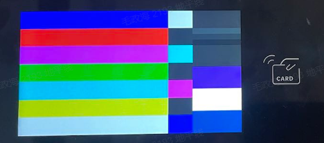
Before using the touchscreen, load the corresponding driver (e.g., gt9xx.ko). Refer to the touchscreen user manual and Driver Development Guide for detailed driver development.
Example of driver loading:
root@buildroot:~$ modprobe gt9xx_core

[   31.725453] Gt9xx driver installing..
[   31.725836] goodix-ts 4-0014: GTP Driver Version: V2.8.1<2022/07/25>
[   31.725846] goodix-ts 4-0014: GTP I2C Address: 0x14
[   31.725858] goodix-ts 4-0014: Unset touchscreen-max-id, use default
[   31.725867] goodix-ts 4-0014: Unset touchscreen-max-w, use default
[   31.725872] goodix-ts 4-0014: Unset touchscreen-max-p, use default
[   31.725879] goodix-ts 4-0014: touch input parameters is [id x y w p]<16 720 1280 1024 1024>
[   31.725892] goodix-ts 4-0014: int-sync enabled
[   31.725897] goodix-ts 4-0014: driver-send-cfg enabled
[   31.725954] goodix-ts 4-0014: Looking up vdd_ana-supply from device tree
[   31.725963] goodix-ts 4-0014: Looking up vdd_ana-supply property in node /soc/a55_apb0/i2c@340f0000/gt9xx@14 failed
[   31.725994] goodix-ts 4-0014: supply vdd_ana not found, using dummy regulator
[   31.733294] goodix-ts 4-0014: Looking up vcc_i2c-supply from device tree
[   31.733304] goodix-ts 4-0014: Looking up vcc_i2c-supply property in node /soc/a55_apb0/i2c@340f0000/gt9xx@14 failed
[   31.733353] goodix-ts 4-0014: supply vcc_i2c not found, using dummy regulator
[   31.740584] goodix-ts 4-0014: Success request irq-gpio
[   31.740606] goodix-ts 4-0014: Success request rst-gpio
[   31.740615] goodix-ts 4-0014: Guitar reset
[   31.770464] do irq down
[   31.833945] goodix-ts 4-0014: I2C Addr is 14
[   31.834979] goodix-ts 4-0014: IC Version: 911_1060
[   31.837180] goodix-ts 4-0014: Config group0 used,length: 186
[   31.839372] goodix-ts 4-0014: Driver send config
[   31.872342] goodix-ts 4-0014: Use slot report protocol
[   31.872888] input: goodix-ts as /devices/virtual/input/input1
[   31.873593] goodix-ts 4-0014: INT num 77, trigger type:2
[   31.873991] goodix-ts 4-0014: create proc entry gt9xx_config success
[   31.874016] goodix-ts 4-0014: Alloc memory size:3070.
[   31.874023] goodix-ts 4-0014: I2C function: without pre and end cmd!
[   31.874032] goodix-ts 4-0014: Create proc entry success!
After successful driver loading, the /dev/input/event1 device node will be created for user-space applications.
Testing Usage:
Use the tc_test program to test touchscreen functionality. When touching the screen, events, types, status codes, and coordinates will be captured.
# ./tc_test /dev/input/event1
Monitoring input events on /dev/input/event1
[/dev/input/event1] event(0): type:3; code: 47; value:  0; realx:  0; realy:  0
[/dev/input/event1] event(1): type:3; code: 57; value: 16; realx:  0; realy:  0
[/dev/input/event1] event(2): type:3; code: 53; value:248; realx:248; realy:  0
[/dev/input/event1] event(3): type:3; code: 54; value:1007; realx:248; realy:1007
[/dev/input/event1] event(4): type:3; code: 48; value: 13; realx:248; realy:1007
[/dev/input/event1] event(5): type:3; code: 58; value: 13; realx:248; realy:1007
Test Code:
#include <stdio.h>
#include <stdlib.h>
#include <fcntl.h>
#include <unistd.h>
#include <linux/input.h>

static int handle_event(int fd, const char *device_name)
{
	struct input_event ev[64];
	int button = 0, realx = 0, realy = 0, i, rd;

	rd = read(fd, ev, sizeof(struct input_event) * 64);
	if (rd < (int)sizeof(struct input_event)) return 0;

	for (i = 0; i < rd / (int)sizeof(struct input_event); i++)
	{
		if (EV_ABS == ev[i].type)
		{
			if (ev[i].code == 53) {
				realx = ev[i].value;
			} else if (ev[i].code == 54) {
				realy = ev[i].value;
			}
		}
		printf("[%s] event(%d): type:%d; code:%3d; value:%3d; realx:%3d; realy:%3d\n",
			   device_name, i, ev[i].type, ev[i].code, ev[i].value, realx, realy);
	}
	return 1;
}

int main(int argc, char *argv[])
{
	if (argc < 2) {
		printf("Usage: %s <event device path>\n", argv[0]);
		return -1;
	}

	const char *device_path = argv[1];
	int fd = open(device_path, O_RDONLY);
	if (fd < 0) {
		printf("Failed to open input device: %s\n", device_path);
		return -1;
	}

	printf("Monitoring input events on %s\n", device_path);
	while (handle_event(fd, device_path));

	close(fd);
	return 0;
}
2.1.3.10. Independent I2C Interface
The development board supports 1 independent I2C interface (interface 25). This interface is primarily designed to work with the MIPI CSI expansion board to split the MIPI CSI0&1 interface (interface 20) into two separate MIPI CSI0 and MIPI CSI1 interfaces. It can also be used as a standalone I2C interface for connecting peripherals.
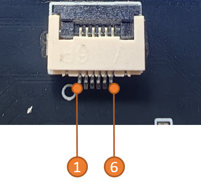
Pin layout is as follows:
| No. | Name | Property | Description |
|---|---|---|---|
| 1 | GND | Signal ground reference | Ground |
| 2 | RESET | 1.8V single-ended output | Board resets module, active low |
| 3 | I2C1_SCL | Default 3.3V single-ended | I2C clock line |
| 4 | I2C1_SDA | Default 3.3V single-ended | I2C data line |
| 5 | CSI1 Triggle | 1.8V single-ended input | Used for triggering Camera Sensor when expanding MIPI CSI1 |
| 6 | VDD33 | 3.3V, 200mA | Module power supply |
2.1.3.11. Wi-Fi / Bluetooth
Using Wi-Fi
The development board integrates the CDW-47852BS dual-mode 2.4G/5.0G Wi-Fi/Bluetooth module, supporting 802.11 b/g/n and Bluetooth 5.1. The Wi-Fi driver is automatically loaded at system startup.
root@buildroot:~$ ifconfig wlan0
wlan0: flags=4098<BROADCAST,MULTICAST>  mtu 1500
        ether 40:9c:a7:70:98:cc  txqueuelen 1000  (Ethernet)
        RX packets 0  bytes 0 (0.0 B)
        RX errors 0  dropped 0  overruns 0  frame 0
        TX packets 0  bytes 0 (0.0 B)
        TX errors 0  dropped 0 overruns 0  carrier 0  collisions 0
Users must manually configure the SSID and IP acquisition by modifying configuration files:
# Enter userdata directory to avoid write errors in system directories
cd /userdata/
# Modify the SSID and password ("WIFI_SSID", "WIFI_PASSWD") according to your Wi-Fi network
wpa_passphrase "WIFI_SSID" "WIFI_PASSWD"  >> ./wpa_supplicant.conf

sleep 1
wpa_supplicant -D nl80211 -i wlan0 -c ./wpa_supplicant.conf -B
sleep 1
udhcpc -i wlan0 &
After configuration, run ping 8.8.8.8 to verify network connectivity. Expected log output:
root@buildroot:~$ cd /userdata/
root@buildroot:/userdata$ wpa_passphrase WiFi-Test 12345678 >> ./wpa_supplicant.conf
root@buildroot:/userdata$ wpa_supplicant -D nl80211 -i wlan0 -c ./wpa_supplicant.conf -B
Successfully initialized wpa_supplicant
[10093.447698] [BB][halbb_la_bb_set_smp_rate] smp_rate_tmp=7, la_smp_rate_log=160 M
root@buildroot:/userdata$ udhcpc -i wlan0 &
[1] 1309
udhcpc: started, v1.35.0
root@buildroot:/userdata$ udhcpc: broadcasting discover
udhcpc: broadcasting select for 192.168.137.252, server 192.168.137.1
udhcpc: lease of 192.168.137.252 obtained from 192.168.137.1, lease time 604800
deleting routers
adding dns 192.168.137.1

[1]+  Done                    udhcpc -i wlan0
root@buildroot:/userdata$ ifconfig wlan0
wlan0: flags=4163<UP,BROADCAST,RUNNING,MULTICAST>  mtu 1500
        inet 192.168.137.252  netmask 255.255.255.0  broadcast 192.168.137.255
        ether 40:9c:a7:70:98:cc  txqueuelen 1000  (Ethernet)
        RX packets 117  bytes 15326 (14.9 KiB)
        RX errors 0  dropped 1  overruns 0  frame 0
        TX packets 63  bytes 5056 (4.9 KiB)
        TX errors 0  dropped 0 overruns 0  carrier 0  collisions 0

root@buildroot:/userdata$ ping 8.8.8.8
PING 8.8.8.8 (8.8.8.8): 56 data bytes
64 bytes from 8.8.8.8: seq=0 ttl=52 time=82.124 ms

64 bytes from 8.8.8.8: seq=1 ttl=52 time=106.029 ms
64 bytes from 8.8.8.8: seq=2 ttl=52 time=129.993 ms
^ C
--- 8.8.8.8 ping statistics ---
3 packets transmitted, 3 packets received, 0% packet loss
round-trip min/avg/max = 82.124/106.048/129.993 ms
root@buildroot:/userdata$
Wi-Fi STA and AP Mode Switching
Run /etc/init.d/wifi_init.sh ap to switch to AP mode, and run /etc/init.d/wifi_init.sh sta to switch to STA mode.
root@buildroot:~# /etc/init.d/wifi_init.sh ap
Initialize wlan0 to ap mode
wlan0: interface state UNINITIALIZED->ENABLED
wlan0: AP-ENABLED
Finish initialize wlan0 to ap mode
dnsmasq: started, version 2.86 cachesize 150
root@buildroot:~# dnsmasq: compile time options: IPv6 GNU-getopt DBus no-UBus no-i18n no-IDN DHCP DHCPv6 no-Lua TFTP no-conntrack ipset auth no-cryptohash no-DNSSEC loop-detect inotify dumpfile
dnsmasq: warning: no upstream servers configured
dnsmasq-dhcp: DHCP, IP range 192.168.5.2 -- 192.168.5.254, lease time 12h
dnsmasq: read /etc/hosts - 2 addresses

root@buildroot:~# /etc/init.d/wifi_init.sh sta
Initialize wlan0 to station mode
Finish initialize wlan0 to station mode
Using Bluetooth
Run /etc/init.d/bt_init.sh to complete Bluetooth initialization.
Run bluetoothctl to enter the interactive Bluetooth configuration interface. If device information similar to the image below appears, the Bluetooth module has been recognized. Use the show command to view Bluetooth details, paying attention to the powered and discoverable status.
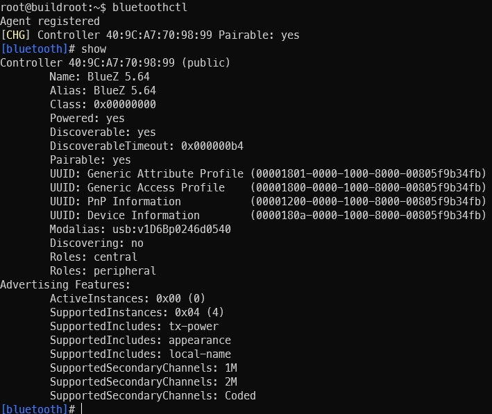
Run power on to enable Bluetooth, as shown below:

To make the Bluetooth device discoverable by nearby devices, run discoverable on to enable the discoverable attribute, as shown below:

At this point, scanning with a phone or computer will reveal a Bluetooth device named “BlueZ 5.64” (the version number may vary depending on the BlueZ version, e.g., it could be BlueZ 5.79):
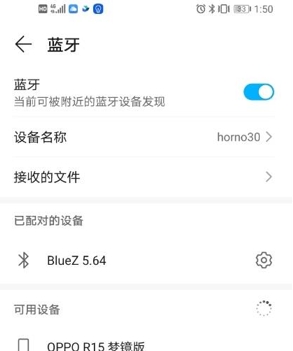
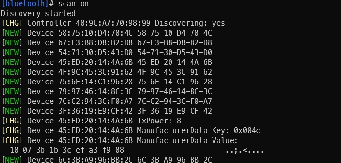
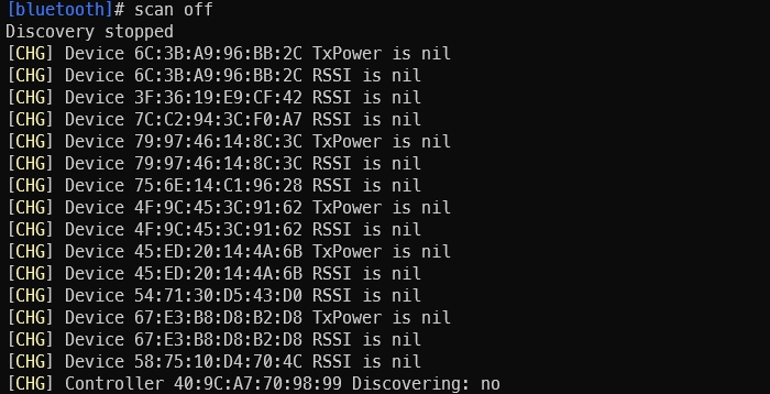
Next, test Bluetooth’s active scanning function. Enter scan on in the bluetoothctl interactive interface to start scanning. It will periodically print nearby devices. As shown, your phone can be detected. Use scan off to stop scanning and summarize the discovered Bluetooth devices:
Then proceed with pairing with other Bluetooth devices:
Pairing command: pair [targetMAC]. After entering the command, confirm with yes when prompted, and select the “Pair” option on the remote Bluetooth device to complete pairing.
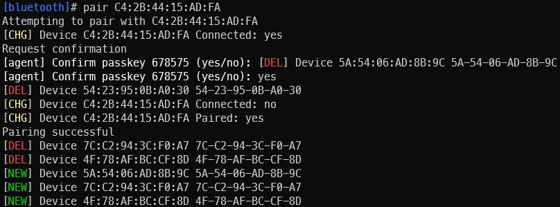
After successful pairing, use trust [targetMAC] to allow automatic connection in the future.
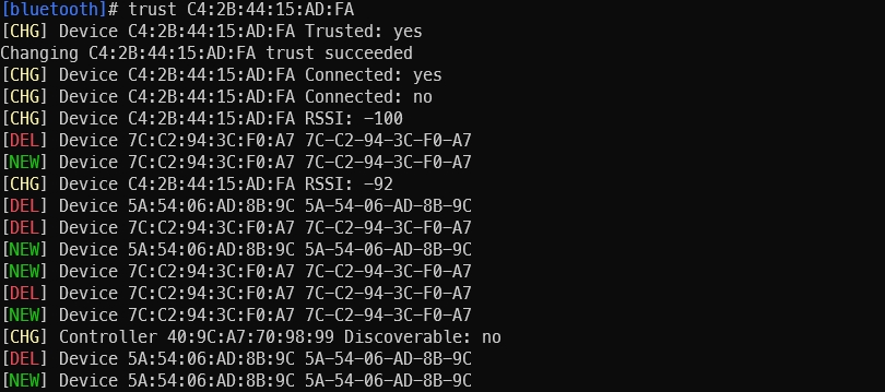
Use l2ping to test network connectivity.

2.1.3.12. TF Card
The development board supports one TF card interface (Connector 26), with maximum support for SDR104 mode. Supported file system formats include FAT32 (VFAT), EXFAT, ext2, ext3, and ext4.
After inserting the TF card, the kernel logs below indicate successful recognition:
[ 9809.931894] mmc1: new HSSDHC card at address 1234
[ 9809.933740] mmcblk1: mmc1:1234 SA16G 14.5 GiB
[ 9809.940060]  mmcblk1: p1
Note: Actual log output may vary slightly depending on the specific model and partitioning of the TF card.
If the file system format on the TF card is not FAT32 (VFAT), ext2, ext3, or ext4, use the following commands to format the TF card partition:
# Format as FAT32 (VFAT)
mkfs.vfat /dev/mmcblk2p1
# Format as ext4
mkfs.ext4 /dev/mmcblk2p1
# Format as ext3
mkfs.ext3 /dev/mmcblk2p1
# Format as ext2
mkfs.ext2 /dev/mmcblk2p1
2.1.3.13. 40-Pin Interface
The development board provides one 40-pin interface (Connector 24) for easy peripheral expansion. The pinout and supported multiplexing functions are shown below:
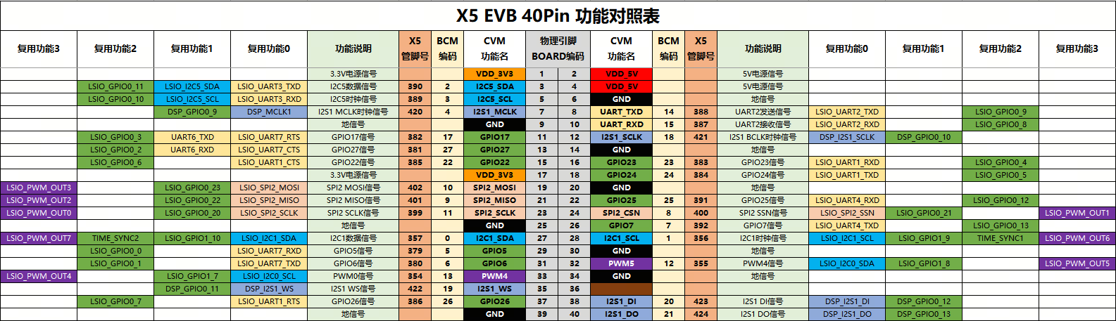
All IO pins on the 40-pin interface default to the 3.3V voltage domain. You can adjust resistors R903 and R902 to switch between 3.3V and 1.8V voltage domains.
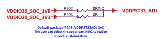
Warning: U-Boot code must be updated synchronously when switching voltage domains. Failure to do so may result in mismatch between software configuration and actual power supply, potentially causing chip damage.
Connection Example:
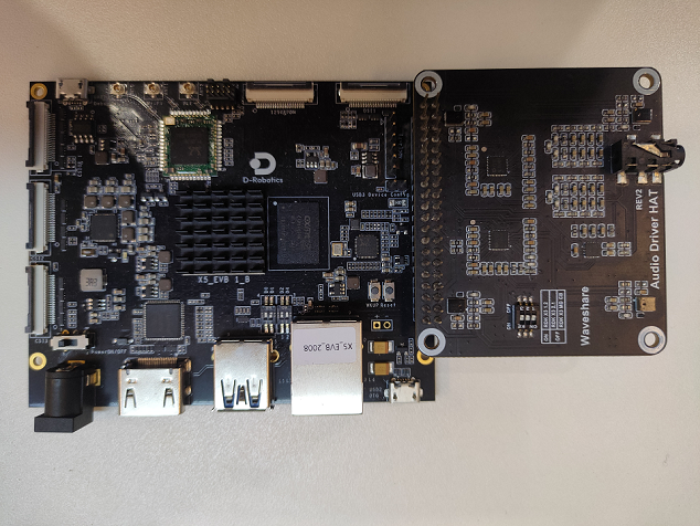
Below is a hardware reference connection diagram for an Audio Driver HAT:
2.1.3.14. RTC Interface
The development board uses an external RTC circuit and battery to maintain system time after power-off. The RTC battery interface (Connector 8) is defined as follows:
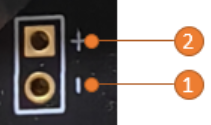
| No. | Name | Description |
|---|---|---|
| 1 | GND | Battery negative, reference ground |
| 2 | VRTC | Battery positive, 3.3V |
The external RTC is enabled by default, and the system automatically loads the RTC chip (PCF8563T) driver. Note: The external battery must be sufficiently charged for proper operation.
After booting, check the startup logs to see the PCF8563T driver messages:
root@buildroot:~# dmesg | grep rtc
……
[    1.508638] rtc-pcf8563 4-0051: pcf8563_probe
[    1.518422] rtc rtc1: read_time: fail to read: -22
[    1.518656] rtc-pcf8563 4-0051: char device (253:1)
[    1.518667] rtc-pcf8563 4-0051: registered as rtc1
From the logs, you can see that pcf8563 is registered as rtc1. Use the following commands to test the external RTC:
# Confirm existence of /dev/rtc1 device
ls /dev/rtc*

# Create a symbolic link from /dev/rtc1 to /dev/rtc
rm /dev/rtc
ln -s /dev/rtc1 /dev/rtc

# Write time to external RTC
date -s "2024/01/01 17:08:00"    # Set system time
hwclock -w                       # Write system time to RTC
hwclock -r                       # Read RTC time to verify write success

# After reboot, read time from external RTC to system
# Confirm existence of /dev/rtc1 device
ls /dev/rtc*
# Create symbolic link from /dev/rtc1 to /dev/rtc
rm /dev/rtc
ln -s /dev/rtc1 /dev/rtc
hwclock -s                               # If RTC battery is present, power cycling will update system time from RTC
date                                     # Read system time, which should now be "2024/01/01 17:08:00"
Now, rechecking the pcf8563 logs shows the time reading process:
# Log after writing time to PCF8563T and rebooting
root@buildroot:~# dmesg | grep rtc
……
[    1.490904] rtc-pcf8563 4-0051: pcf8563_probe
[    1.492784] rtc-pcf8563 4-0051: pcf8563_rtc_read_time: raw data is st1=08, st2=00, sec=35, min=08, hr=17, mday=01, wday=31, mon=21, year=24
[    1.492805] rtc-pcf8563 4-0051: pcf8563_rtc_read_time: tm is secs=35, mins=8, hours=17, mday=1, mon=0, year=124, wday=1
[    1.493485] rtc-pcf8563 4-0051: pcf8563_rtc_read_alarm: raw data is min=80, hr=9c, mday=90, wday=94
[    1.493902] rtc-pcf8563 4-0051: pcf8563_rtc_read_alarm: tm is mins=0, hours=22, mday=10, wday=4, enabled=0, pending=0
[    1.495035] rtc-pcf8563 4-0051: pcf8563_rtc_read_time: raw data is st1=08, st2=00, sec=35, min=08, hr=17, mday=01, wday=31, mon=21, year=24
[    1.495055] rtc-pcf8563 4-0051: pcf8563_rtc_read_time: tm is secs=35, mins=8, hours=17, mday=1, mon=0, year=124, wday=1
[    1.496190] rtc-pcf8563 4-0051: pcf8563_rtc_read_time: raw data is st1=08, st2=00, sec=35, min=08, hr=17, mday=01, wday=31, mon=21, year=24
[    1.496213] rtc-pcf8563 4-0051: pcf8563_rtc_read_time: tm is secs=35, mins=8, hours=17, mday=1, mon=0, year=124, wday=1
[    1.496465] rtc-pcf8563 4-0051: char device (253:1)
[    1.496481] rtc-pcf8563 4-0051: registered as rtc1
2.1.3.15. ADC Interface
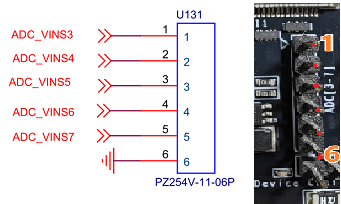
Connector 11 is the ADC (Analog-to-Digital Converter) interface on the development board. It provides five pins labeled ADC[3-7] for connecting analog signal sources and converting them into digital signals for system processing. Users can read corresponding system files to obtain the converted ADC values.
Input Voltage Range: The supported input voltage range is 0.1–1.7V. Ensure that the input signal voltage stays within this range to avoid signal distortion or ADC damage.
Reading ADC Values
Read the system files /sys/bus/iio/devices/iio:device0/in_voltage3_raw to /sys/bus/iio/devices/iio:device0/in_voltage7_raw to get the raw ADC values for channels ADC[3-7]. For example, to read ADC3 value:
root@buildroot:~$ cat /sys/bus/iio/devices/iio:device0/in_voltage3_raw
1020
This command outputs the raw digital value from the ADC3 channel. To read values from ADC[3-7], simply replace in_voltage3_raw with the corresponding in_voltageX_raw (where X ranges from 3 to 7).
2.1.3.16. Other Interfaces
Power Switch
Controls power-on and power-off of the board. Corresponds to Connector 23.
Reset Switch
Resets the board by pulling down the chip’s RSTN signal. Corresponds to Connector 6.
Wake-up Switch
Used to wake up the system from Sleep mode via an external wake-up source. Corresponds to Connector 7.
JTAG Debug Interface
Used with tools like DS5 for chip debugging. Corresponds to Connector 14. The connector is not pre-soldered on the board; manual soldering is required before use.