7.4. Overview of Journey 5
Journey 5 (J5) is an AD-specific (autonomous driving specific) chip algorithm processor with low power consumption and high-performance launched by Horizon Robotics in 2021.
In terms of computing power, J5 is equipped with 8-core Cortex-A55 CPU, dual-core Vision P6 DSP, and dual-core BPU (Brain Processing Unit) chip algorithm processor. The BPU accelerator is designed with a new generation of Bayes architecture that provides 128 TOPS of BPU computing power.
Note
The BPU is an acceleration core developed by Horizon Robotics. With the scenarios requirements of autonomous driving in the design process, it performs collaborative optimization of software and hardware architecture at three aspects: algorithms, computing architecture, and compiler, which improves several times of the computing power performance with no change in power consumption.
The J5 processor has a built-in BPU core with Bayes architecture, which greatly improves the support for advanced CNN networks and reduces the DDR bandwidth usage. It also provides the capabilities such as real-time pixel-level video segmentation and structured video analysis.
In terms of image processing capability, the J5 processor includes two high-performance ISP image processing modules, each of which supports 2x4k/8M@30fps image processing, multi-frame exposure wide dynamic (HDR), and provides high quality images in terrible lighting scenes. The ISP module also supports various mainstream CFAs, such as RGGB, RCCC, RGBIR 2x2, RCCB, RCCG and RYYCy, etc.
The J5 ISP also supports features including black level correction, defective pixel detection and correction, spatial noise reduction, chromatic aberration correction, lens shading correction, demosaicing, etc. We also offer some proprietary ISP modification tools for the customers to adjust ISP parameters and image effects.
Please contact Horizon technical supports or sales if you have any questions.
For better usage of the J5’s chip algorithm capabilities, you will get complete development board kits, chip algorithm development platforms, and various AD solutions based on the J5.
You can refer to the following relevant sections for more information.
The following sections describes the system-on-chip and peripherals of the J5 processor.
7.4.1. SoC
The functional block diagram of the processor is shown in the following figure:
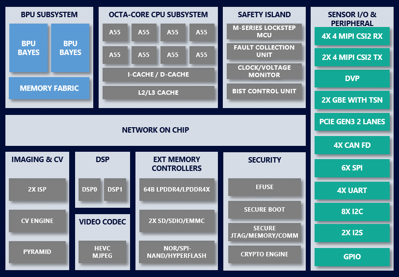
CPU: J5 processor uses an octa-core Cortex-A55 as the main CPU.
BPU: J5 processor uses the dual-core BPU with Horizon Gen-3 Bayes architecture.
DSP: J5 processor contains two programmable Vision P6 DSP modules, which can be used for CV calculation acceleration, which can also be used for neural network computation. The DSP supports SIMD and VLIW computing architectures to improve computing efficiency, with frequencies up to 650 MHz. The DSP can be configured to 256 8x8 MACs for a total of 0.67 TOPS.
Note
The two built-in BPU cores in the J5 processor provide pretty flexible multi-core scheduling capabilities for model scheduling at the business level.
Single Frame & Single Core: By manually scheduling a single model inference to a single BPU core, the high-priority models for full-image detection can be physically isolated from the low-priority models for scenarios such as detection + classification.
In the case where resources such as DDR has not yet reached the bottleneck, single frame single core can guarantee the isolation of the scheduling and inference on two BPU cores.
Multi-threaded, Multi-frame, Dual-core: This scenario can double the inference FPS. However, for larger models, multi-threaded, multi-frame, and dual-core may not be able to double the FPS due to the consumption of dual-core scheduling.
For more technical details on how to efficiently use the dual-core BPU, refer to BPU SDK API Manual.
J5 SoC launched by Horizon Robotics is designed in strict compliance with functional safety requirements and procedures, integrating multiple safety mechanisms for fast detection and response to hardware failures, which complies with ASIL-B standards.
7.4.2. On-chip Peripherals Interfaces
Support 4× 2.5G MIPI CSI RX
Support 2× 2.5G MIPI CSI TX
Support 1× DVP
Support 8× I2C
Support 4× SPI master and 2× SPI slave, with 1× SPI master and 1× SPI slave multiplexed
Support 4× UART
Support 4× CANF-FD
Support 2× 1Gb Ethernet, with eth0 supporting TSN
Support 1× PCIe Gen3 2-Lane
Support 16 LPWM and 2× PWM
Support 1× eMMC and 1× SD/SDIO
Support 1× OSPI to connect NOR/Hyper/NAND flash
Support 64bit LPDDR4/4X memory
Support 2× I2S